|
Os motores de busca de Datasheet de Componentes eletrônicos |
|
|
Os motores de busca de Datasheet de Componentes eletrônicos |
|
11C90DC Folha de dados(PDF) 6 Page - National Semiconductor (TI) |
|
|
|
|||||||||||||||||||||||||||||
11C90DC Folha de dados(HTML) 6 Page - National Semiconductor (TI) |
|
|
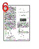
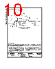
6 / 10 page  Functional Description The 11C90 contains four ECL Flip-Flops an ECL to TTL converter and a Schottky TTL output buffer with an active pull-up Three of the Flip-Flops operate as a synchronous shift counter driving the fourth Flip-Flop operating as an asynchronous toggle The internal feedback logic is such that the TTL output and the Q ECL output are HIGH for six clock periods and LOW for five clock periods The Mode Control (M) inputs can modify the feedback to make the output HIGH for five clock periods and LOW for five clock periods as indicated in the Count Sequence Table The feedback logic is such that the instant the output goes HIGH the circuit is already committed as to whether the output period will be 10 or 11 clock periods long This means that subsequent changes in an M input signal in- cluding decoding spikes will have no effect on the current output period The only timing restriction for an M input sig- nal is that it be in the desired state at least a setup time before the clock that follows the HHLL state shown in the table The allowable propagation delay through external log- ic to an M input is maximized by designing it to use the positive transition of the 11C90 output as its active edge This gives an allowable delay of ten clock periods minus the CP to Q delay of the 11C90 and the M to CP setup time If the external logic uses the negative output transition as its active edge the allowable delay is reduced to five clock periods minus the previously mentioned delay and setup time Capacitively coupled triggering is simplified by the 400X re- sistor which connects pin 15 to the internal VBB reference By connecting this to the CP input as shown in Figure 3 the clock is automatically centered about the input threshold A clock duty cycle of 50% provides the fastest operation since the Flip-Flops are Master-Slave types with offset clock thresholds between master and slave This feature ensures that the circuit will operate with clock waveforms having very slow rise and fall times and thus there is no maximum frequency restriction Recommended minimum and maxi- mum clock amplitude as a function of a frequency and tem- perature are shown in the graph labeled Figure 2 When the CP or any other input is driven from another ECL circuit normal ECL termination methods are recommended One method is indicated in Figure 4 Other ECL termination methods are discussed in the F100K ECL Design Guide (Section 5 of Databook) TLF9892 – 5 FIGURE 2 AC Coupled Triggering Characteristics TLF9892 – 10 FIGURE 3 Capacitively Coupled Clocking TLF9892 – 11 ZOX 50 75 100 R1X 806 121 162 R2X 130 196 261 VEE eb52V VCC e 0V VTT eb20V FIGURE 4 Clocking by ECL Source via Terminated Line When an M input is to be driven from a TTL output operating from the same VCC and ground (VEE) the internal 2 kX resistor can be used to pull the TTL output up as shown in Figure 5 Some types of TTL outputs will only pull up to within two diode drops of VCC which is not high enough for 11C90 inputs The resistor will pull the signal up through the threshold region although this final rise may be somewhat slow depending on wiring capacitance A resistor network that gives faster rise and also lower impedance is shown in Figure 6 TLF9892 – 12 FIGURE 5 Using Internal Pull-Up with TTL Source TLF9892 – 13 FIGURE 6 Faster Low Impedance TTL to ECL Interface 6 |
|
|
Ligação URL |
| ALLDATASHEET é útil para você? [ DONATE ] |
Sobre Alldatasheet | Publicidade | Contato conosco | Privacy Policy | Link para a ficha técnica | roca de Link | Lista de Fabricantes All Rights Reserved©Alldatasheet.com |
| Russian : Alldatasheetru.com | Korean : Alldatasheet.co.kr | Spanish : Alldatasheet.es | French : Alldatasheet.fr | Italian : Alldatasheetit.com Portuguese : Alldatasheetpt.com | Polish : Alldatasheet.pl | Vietnamese : Alldatasheet.vn Indian : Alldatasheet.in | Mexican : Alldatasheet.com.mx | British : Alldatasheet.co.uk | New Zealand : Alldatasheet.co.nz |
|
Family Site : ic2ic.com |
icmetro.com |
 Portuguese ▼
 English
 Chinese
 German
 Japanese
 Russian
 Korean
 Spanish
 French
 Italian
 Portuguese
 Polish
 Vietnamese
 Indian
 Mexican
 British
 New Zealand