|
Os motores de busca de Datasheet de Componentes eletrônicos |
|
|
Os motores de busca de Datasheet de Componentes eletrônicos |
|
MSK738 Folha de dados(PDF) 3 Page - M.S. Kennedy Corporation |
|
|
|||||||||||||||||||||||||||||
MSK738 Folha de dados(HTML) 3 Page - M.S. Kennedy Corporation |
|
|
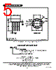
3 / 5 page  APPLICATION NOTES HEAT SINKING To determine if a heat sink is necessary for your application and if so, what type, refer to the thermal model and governing equation below. Governing Equation: Example: This example demonstrates a worst case analysis for the op-amp output stage. This occurs when the output voltage is 1/2 the power supply voltage. Under this condition, maximum power transfer oc- curs and the output is under maximum stress. Conditions: VCC=±16VDC VO=±8Vp Sine Wave, Freq.=1KHz RL=100 Ω For a worst case analysis we will treat the +8Vp sine wave as an 8VDC output voltage. 1.) Find Driver Power Dissipation PD=(VCC-VO) (VO/RL) =(16V-8V) (8V/100 Ω) =0.64W 2.) For conservative design, set TJ=+125°C 3.) For this example, worst case TA=+90°C 4.) R θJC=46°C/W from MSK 738B Data Sheet 5.) R θCS=0.15°C/W for most thermal greases 6.) Rearrange governing equation to solve for R θSA R θSA=((TJ-TA)/PD) - (RθJC) - (RθCS) =((125°C -90°C)/0.64W) - 45°C/W - 0.15°C/W =54.7 - 46.15 =8.5°C/W Rev. C 9/06 3 TJ=PD x (R θJC + RθCS + RθSA) + TA Where TJ=Junction Temperature PD=Total Power Dissipation R θJC=Junction to Case Thermal Resistance R θCS=Case to Heat Sink Thermal Resistance R θSA=Heat Sink to Ambient Thermal Resistance TC=Case Temperature TA=Ambient Temperature TS=Sink Temperature Potentiometer values ranging from 1K Ω to 1MΩ can be used with only a small amount of degradation (typically 0.15 to 0.25µV/°C) of input offset voltage drift. If the input offset voltage is to be trimmed to a value other than "zero", the following formula can be used to approximate the change in input offset voltage drift: ∆VOSD=VOS (trimmed)/250 Recommended External Component Selection Guide APPROXIMATE DESIRED GAIN RI(+) RI(-) Rf(Ext) Cf -1 499 Ω 1K Ω 1K Ω -2 330 Ω 499 Ω 1K Ω -5 169 Ω 200 Ω 1K Ω -8 100 Ω 124 Ω 1K Ω 90.9 Ω 100 Ω 1K Ω -20 -10 100 Ω 100 Ω 2K Ω 1 The positive input resistor is selected to minimize any bias current induced offset voltage. 2 The feedback capacitor will help compensate for stray input capacitance. The value of this capacitor can be dependent on individual applications. A 2 to 9 pf capacitor is usually optimum for most applications. Thermal Model: The heat sink in this example must have a thermal resistance of no more than 8.5°C/W to maintain a junction temperature of no more than +125°C. OFFSET NULL Typically, the MSK 738(B) has an input offset voltage of less than ±25µV. If it is desirable to adjust the offset closer to "zero", or to a value other than "zero", the circuit below is recommended. RP should be a ten-turn 10K Ω potentiometer. Typical offset adjust is ±5mV. 2 2 2 2 2 2 1 1 1 1 1 1 1µf 1µf 1µf 1µf 1µf 1µf C1 |
|
|
Ligação URL |
| ALLDATASHEET é útil para você? [ DONATE ] |
Sobre Alldatasheet | Publicidade | Contato conosco | Privacy Policy | Link para a ficha técnica | roca de Link | Lista de Fabricantes All Rights Reserved©Alldatasheet.com |
| Russian : Alldatasheetru.com | Korean : Alldatasheet.co.kr | Spanish : Alldatasheet.es | French : Alldatasheet.fr | Italian : Alldatasheetit.com Portuguese : Alldatasheetpt.com | Polish : Alldatasheet.pl | Vietnamese : Alldatasheet.vn Indian : Alldatasheet.in | Mexican : Alldatasheet.com.mx | British : Alldatasheet.co.uk | New Zealand : Alldatasheet.co.nz |
|
Family Site : ic2ic.com |
icmetro.com |
 Portuguese ▼
 English
 Chinese
 German
 Japanese
 Russian
 Korean
 Spanish
 French
 Italian
 Portuguese
 Polish
 Vietnamese
 Indian
 Mexican
 British
 New Zealand