|
Os motores de busca de Datasheet de Componentes eletrônicos |
|
|
Os motores de busca de Datasheet de Componentes eletrônicos |
|
MP4603 Folha de dados(PDF) 12 Page - Monolithic Power Systems |
|
|
|||||||||||||||||||||||||||||
MP4603 Folha de dados(HTML) 12 Page - Monolithic Power Systems |
|
|
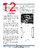
12 / 18 page  MP4603 – WHITE LED DRIVER FOR LARGE SIZE TV BACKLIGHTING MP4603 Rev. 1.0 www.MonolithicPower.com 12 4/27/2012 MPS Proprietary Information. Patent Protected. Unauthorized Photocopy and Duplication Prohibited. © 2012 MPS. All Rights Reserved.MP4603 Selecting the Output Capacitor The output capacitor normally limits the output voltage ripple ( VOUT) to less than 1%-to-5% of the DC value, and ensures a stable feedback loop. Select an output capacitor value with low impedance at the switching frequency. Use ceramic capacitors with X5R or X7R dielectrics for their low ESR characteristics. LED OUT OUT sOUT IN OUT IV C fV (V V ) Setting the Over Voltage Protection The output voltages of some converters, such as buck-boost and boost converters, can rise to very high levels without a limiting function. Over- voltage protection (OVP) limits the output voltage to below the operating rating. Use a voltage divider to set the OVP point. 1 OVP 2 R V1.2V (1 ) R Where R1 and R2 are the voltage divider (refer the TYPICAL APPLICATION). For most applications, set the OVP point around 10% to 30% higher than the output voltage. Check that the set OVP point will not exceed the operation rating. FAULT Condition Output The MP4603 has an open drain output as a FAULT indicator. Under normal conditions, FAULT is a high-Z output and can be set to any desired voltage with external resistors. However, if VFB exceeds VSS by 600mV, or VFB exceeds VSS by 300mV for ~450μs, or OVP triggers at 1.2V, FAULT drops to the INGND level. The Rdson for this pull down switch is ~100Ω. PC Board Layout Place the high-current paths (VSS, VIN and SW) very close to the device with short, direct, and wide traces. Place the input capacitor as close as possible to the VIN and VSS pins. Place the external feedback resistors next to the FB pin. Keep the switch node traces short and far away from the feedback network. Pay attention to the layout of the high frequency switching loop, which should be placed as small as possible. For buck applications, the high frequency switching loop is composed of the input capacitor, the internal switch of IC (VIN pin to SW pin) and the diode. Place the input capacitor and the diode close to the IC. For buck-boost applications, the high frequency switching loop is composed of the input capacitor, the internal switch, the diode and the output capacitor. Place the input and output capacitors close together, close to the IC, and to the diode. Top Layer Bottom Layer Figure 2: PCB Layout |
|
|
Ligação URL |
| ALLDATASHEET é útil para você? [ DONATE ] |
Sobre Alldatasheet | Publicidade | Contato conosco | Privacy Policy | Link para a ficha técnica | roca de Link | Lista de Fabricantes All Rights Reserved©Alldatasheet.com |
| Russian : Alldatasheetru.com | Korean : Alldatasheet.co.kr | Spanish : Alldatasheet.es | French : Alldatasheet.fr | Italian : Alldatasheetit.com Portuguese : Alldatasheetpt.com | Polish : Alldatasheet.pl | Vietnamese : Alldatasheet.vn Indian : Alldatasheet.in | Mexican : Alldatasheet.com.mx | British : Alldatasheet.co.uk | New Zealand : Alldatasheet.co.nz |
|
Family Site : ic2ic.com |
icmetro.com |
 Portuguese ▼
 English
 Chinese
 German
 Japanese
 Russian
 Korean
 Spanish
 French
 Italian
 Portuguese
 Polish
 Vietnamese
 Indian
 Mexican
 British
 New Zealand