|
Os motores de busca de Datasheet de Componentes eletrônicos |
|
|
Os motores de busca de Datasheet de Componentes eletrônicos |
|
MT-059 Folha de dados(PDF) 14 Page - Analog Devices |
|
|
|||||||||||||||||||||||||||||
MT-059 Folha de dados(HTML) 14 Page - Analog Devices |
|
|
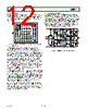
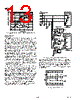
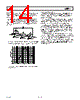
14 / 17 page  AD8044 REV. B –13– Active Filters Active filters at higher frequencies require wider bandwidth op amps to work effectively. Excessive phase shift produced by lower frequency op amps can significantly impact active filter performance. Figure 38 shows an example of a 2 MHz biquad bandwidth filter that uses three op amps of an AD8044 package. Such circuits are sometimes used in medical ultrasound systems to lower the noise bandwidth of the analog signal before A/D conversion. 2 3 1 R1 3k VIN R2 2k C1 50pF R3 2k 6 5 7 R6 1k R5 2k 9 10 8 AD8044 AD8044 AD8044 C2 50pF VOUT R4 2k Figure 38. 2 MHz Biquad Band-pass Filter Using AD8044 The frequency response of the circuit is shown in Figure 39. FREQUENCY (Hz) 0 –10 10k 100M 100k 1M 10M –20 –30 –40 Figure 39. Frequency Response of 2 MHz Band-pass Biquad Filter Layout Considerations The specified high speed performance of the AD8044 requires careful attention to board layout and component selection. Proper RF design techniques and low-pass parasitic component selection are necessary. The PCB should have a ground plane covering all unused por- tions of the component side of the board to provide a low im- pedance path. The ground plane should be removed from the area near the input pins to reduce the stray capacitance. Chip capacitors should be used for the supply bypassing. One end should be connected to the ground plane and the other within 1/8 inch of each power pin. An additional large (0.47 mF – 10 mF) tantalum electrolytic capacitor should be connected in parallel, but not necessarily so close, to supply current for fast, large signal changes at the output. The feedback resistor should be located close to the inverting input pin in order to keep the stray capacitance at this node to a minimum. Capacitance variations of less than 1 pF at the invert- ing input will significantly affect high speed performance. Stripline design techniques should be used for long signal traces (greater than about 1 inch). These should be designed with a characteristic impedance of 50 W or 75 W and properly termi- nated at each end. |
|
|
Ligação URL |
| ALLDATASHEET é útil para você? [ DONATE ] |
Sobre Alldatasheet | Publicidade | Contato conosco | Privacy Policy | Link para a ficha técnica | roca de Link | Lista de Fabricantes All Rights Reserved©Alldatasheet.com |
| Russian : Alldatasheetru.com | Korean : Alldatasheet.co.kr | Spanish : Alldatasheet.es | French : Alldatasheet.fr | Italian : Alldatasheetit.com Portuguese : Alldatasheetpt.com | Polish : Alldatasheet.pl | Vietnamese : Alldatasheet.vn Indian : Alldatasheet.in | Mexican : Alldatasheet.com.mx | British : Alldatasheet.co.uk | New Zealand : Alldatasheet.co.nz |
|
Family Site : ic2ic.com |
icmetro.com |
 Portuguese ▼
 English
 Chinese
 German
 Japanese
 Russian
 Korean
 Spanish
 French
 Italian
 Portuguese
 Polish
 Vietnamese
 Indian
 Mexican
 British
 New Zealand