|
Os motores de busca de Datasheet de Componentes eletrônicos |
|
|
Os motores de busca de Datasheet de Componentes eletrônicos |
|
LTC1296CCSW Folha de dados(PDF) 7 Page - Linear Technology |
|
|
|||||||||||||||||||||||||||||
LTC1296CCSW Folha de dados(HTML) 7 Page - Linear Technology |
|
|
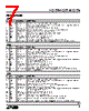
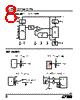
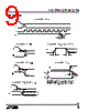
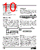
7 / 28 page  7 LTC1293/LTC1294/LTC1296 129346fs PI FU CTIO S # PIN FUNCTION DESCRIPTION 1 – 6 CH0 – CH5 Analog Inputs The analog inputs must be free of noise with respect to AGND. 7 COM Common The common pin defines the zero reference point for all single ended inputs. It must be free of noise and is usually tied to the analog ground plane. 8 DGND Digital Ground This is the ground for the internal logic. Tie to the ground plane. 9V – Negative Supply Tie V – to most negative potential in the circuit (Ground in single supply applications). 10 AGND Analog Ground AGND should be tied directly to the analog ground plane. 11 VREF Ref. Input The reference inputs must be kept free of noise with respect to AGND. 12 DIN Data Input The A/D configuration word is shifted into this input. 13 DOUT Digital Data Output The A/D conversion result is shifted out of this output. 14 CS Chip Select Input A logic low on this input enables data transfer. 15 CLK Clock This clock synchronizes the serial data transfer and controls A/D conversion rate. 16 VCC Positive supply This supply must be kept free of noise and ripple by bypassing directly to the analog ground plane. LTC1293 # PIN FUNCTION DESCRIPTION 1 –8 CH0 – CH7 Analog Inputs The analog inputs must be free of noise with respect to AGND. 9 COM Common The common pin defines the zero reference point for all single ended inputs. It must be free of noise and is usually tied to the analog ground plane. 10 DGND Digital Ground This is the ground for the internal logic. Tie to the ground plane. 11 V – Negative Supply Tie V – to most negative potential in the circuit (Ground in single supply applications). 12 AGND Analog Ground AGND should be tied directly to the analog ground plane. 13, 14 REF –, REF+ Ref. Inputs The reference inputs must be kept free of noise with respect to AGND. The A/D sees a reference voltage equal to the difference between REF + and REF–. 15 DIN Data Input The A/D configuration word is shifted into this input. 16 DOUT Digital Data Output The A/D conversion result is shifted out of this output. 17 CS Chip Select Input A logic low on this input enables data transfer. 18 CLK Clock This clock synchronizes the serial data transfer and controls A/D converion rate. 19, 20 AVCC, DVCC Positive Supplies These supplies must be kept free of noise and ripple by bypassing directly to the analog ground plane. AVCC and DVCC must be tied together. LTC1294 # PIN FUNCTION DESCRIPTION 1 –8 CH0 – CH7 Analog Inputs The analog inputs must be free of noise with respect to AGND. 9 COM Common The common pin defines the zero reference point for all single ended inputs. It must be free of noise and is usually tied to the analog ground plane. 10 DGND Digital Ground This is the ground for the internal logic. Tie to the ground plane. 11 V – Negative Supply Tie V – to most negative potential in the circuit (Ground in single supply applications). 12 AGND Analog Ground AGND should be tied directly to the analog ground plane. 13, 14 REF –, REF+ Ref. Inputs The reference inputs must be kept free of noise with respect to AGND. The A/D sees a reference voltage equal to the difference between REF + and REF–. 15 DIN Data Input The A/D configuration word is shifted into this input. 16 DOUT Digital Data Output The A/D conversion result is shifted out of this output. 17 CS Chip Select Input A logic low on this input enables data transfer. 18 CLK Clock This clock synchronizes the serial data transfer and controls A/D conversion rate. 19 SSO System Shutdown System Shutdown Output pin will go low when power shutdown is requested. Output 20 VCC Positive Supply This supply must be kept free of noise and ripple by bypassing directly to the analog ground plane. LTC1296 |
|
Ligação URL |
| ALLDATASHEET é útil para você? [ DONATE ] |
Sobre Alldatasheet | Publicidade | Contato conosco | Privacy Policy | Link para a ficha técnica | roca de Link | Lista de Fabricantes All Rights Reserved©Alldatasheet.com |
| Russian : Alldatasheetru.com | Korean : Alldatasheet.co.kr | Spanish : Alldatasheet.es | French : Alldatasheet.fr | Italian : Alldatasheetit.com Portuguese : Alldatasheetpt.com | Polish : Alldatasheet.pl | Vietnamese : Alldatasheet.vn Indian : Alldatasheet.in | Mexican : Alldatasheet.com.mx | British : Alldatasheet.co.uk | New Zealand : Alldatasheet.co.nz |
|
Family Site : ic2ic.com |
icmetro.com |
 Portuguese ▼
 English
 Chinese
 German
 Japanese
 Russian
 Korean
 Spanish
 French
 Italian
 Portuguese
 Polish
 Vietnamese
 Indian
 Mexican
 British
 New Zealand