|
Os motores de busca de Datasheet de Componentes eletrônicos |
|
|
Os motores de busca de Datasheet de Componentes eletrônicos |
|
TC7109CLW Folha de dados(PDF) 17 Page - Microchip Technology |
|
|
|||||||||||||||||||||||||||||
TC7109CLW Folha de dados(HTML) 17 Page - Microchip Technology |
|
|
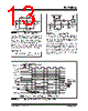
17 / 32 page  2002-2012 Microchip Technology Inc. DS21456D-page 17 TC7109/A 4.0 INTERFACING 4.1 Direct Mode Combinations of chip enable and byte enable control signals, which may be used when interfacing the TC7109A to parallel data lines, are shown in Figure . The CE/LOAD input may be tied low, allowing either byte to be controlled by its own enable (see Figure (A)). Figure (B) shows the HBEN and LBEN as flag inputs, and CE/LOAD as a master enable, which could be the READ strobe available from most microprocessors. Figure (C) shows a configuration where the two byte enables are connected together. The CE/LOAD is a chip enable, and the HBEN and LBEN may be used as a second chip enable, or connected to ground. The 14 data outputs will be enabled at the same time. In the direct MODE, SEND should be tied to V+. Figure shows interfacing several TC7109A’s to a bus, ganging the HBEN and LBEN signals to several converters together, and using the CE/LOAD input to select the desired converter. Figure through Figure give practical circuits utilizing the parallel three-state output capabilities of the TC7109A. Figure shows parallel interface to the 8748/ 49 systems via an 8255 PPI, where the TC7109A data outputs are active at all times. This interface can be used in a read-after-update sequence, as shown in Figure . The data is accessed by the high-to-low transition of the Status driving an interrupt to the microcontroller. The RUN/HOLD input is also used to initiate conversions under software control. Direct interfacing to most microcontroller busses is easily accomplished through the three-state output of the TC7109A. Figure 4-8 is a typical connection diagram. To ensure requirements for setup and hold times, minimum pulse widths, and the drive limitations on long busses are met, it is necessary to carefully consider the system timing in this type of interface. This type of interface is used when the memory peripheral address density is low, providing simple address decoding. Interrupt handling can be simplified by using an interface to reduce the component count. FIGURE 4-1: Direct Mode Chip and Byte Enable Combination TC7109A MODE CE/LOAD B9 - B12 POL, OR B1 - B8 LBEN HBEN GND 8 Analog In 6 Convert Control RUN/HOLD TC7109A MODE CE/LOAD B1 - B12 POL, OR LBEN HBEN GND Analog In Convert RUN/HOLD TC7109A MODE CE/LOAD B9 - B12 POL, OR B1 - B8 LBEN HBEN 8 Analog In 6 Convert RUN/HOLD Chip Select 1 GND or Chip Select 2 14 Byte Flags GND Chip Select A. B. C. |
|
Ligação URL |
| ALLDATASHEET é útil para você? [ DONATE ] |
Sobre Alldatasheet | Publicidade | Contato conosco | Privacy Policy | Link para a ficha técnica | roca de Link | Lista de Fabricantes All Rights Reserved©Alldatasheet.com |
| Russian : Alldatasheetru.com | Korean : Alldatasheet.co.kr | Spanish : Alldatasheet.es | French : Alldatasheet.fr | Italian : Alldatasheetit.com Portuguese : Alldatasheetpt.com | Polish : Alldatasheet.pl | Vietnamese : Alldatasheet.vn Indian : Alldatasheet.in | Mexican : Alldatasheet.com.mx | British : Alldatasheet.co.uk | New Zealand : Alldatasheet.co.nz |
|
Family Site : ic2ic.com |
icmetro.com |
 Portuguese ▼
 English
 Chinese
 German
 Japanese
 Russian
 Korean
 Spanish
 French
 Italian
 Portuguese
 Polish
 Vietnamese
 Indian
 Mexican
 British
 New Zealand