|
Os motores de busca de Datasheet de Componentes eletrônicos |
|
|
Os motores de busca de Datasheet de Componentes eletrônicos |
|
AD9767 Folha de dados(PDF) 15 Page - Analog Devices |
|
|
|||||||||||||||||||||||||||||
AD9767 Folha de dados(HTML) 15 Page - Analog Devices |
|
|
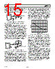
15 / 27 page  REV. B AD9767 –15– IOUTFS and RLOAD can be selected as long as the positive compli- ance range is adhered to. One additional consideration in this mode is the integral nonlinearity (INL) as discussed in the Analog Output section of this data sheet. For optimum INL performance, the single-ended, buffered voltage output configu- ration is suggested. AD9767 IOUTA IOUTB 50 25 50 VOUTA = 0 TO +0.5V IOUTFS = 20mA Figure 36. 0 V to 0.5 V Unbuffered Voltage Output SINGLE-ENDED, BUFFERED VOLTAGE OUTPUT CONFIGURATION Figure 37 shows a buffered single-ended output configuration in which the op amp U1 performs an I-V conversion on the AD9767 output current. U1 maintains IOUTA (or IOUTB) at a virtual ground, thus minimizing the nonlinear output impedance effect on the DAC’s INL performance as discussed in the Analog Output section. Although this single-ended configura- tion typically provides the best dc linearity performance, its ac distortion performance at higher DAC update rates may be limited by U1’s slewing capabilities. U1 provides a negative unipolar output voltage and its full-scale output voltage is sim- ply the product of RFB and IOUTFS. The full-scale output should be set within U1’s voltage output swing capabilities by scaling IOUTFS and/or RFB. An improvement in ac distortion perfor- mance may result with a reduced IOUTFS since the signal current U1 will be required to sink will be subsequently reduced. AD9767 IOUTA IOUTB COPT 200 U1 VOUT = IOUTFS RFB IOUTFS = 10mA RFB 200 Figure 37. Unipolar Buffered Voltage Output POWER AND GROUNDING CONSIDERATIONS, POWER SUPPLY REJECTION Many applications seek high speed and high performance under less than ideal operating conditions. In these application cir- cuits, the implementation and construction of the printed circuit board is as important as the circuit design. Proper RF tech- niques must be used for device selection, placement and rout- ing, as well as power supply bypassing and grounding to ensure optimum performance. Figures 43 to 50 illustrate the recom- mended printed circuit board ground, power and signal plane layouts which are implemented on the AD9767 evaluation board. One factor that can measurably affect system performance is the ability of the DAC output to reject dc variations or ac noise superimposed on the analog or digital dc power distribution. This is referred to as the Power Supply Rejection Ratio. For dc variations of the power supply, the resulting performance of the DAC directly corresponds to a gain error associated with the DAC’s full-scale current, IOUTFS. AC noise on the dc supplies is common in applications where the power distribution is gener- ated by a switching power supply. Typically, switching power supply noise will occur over the spectrum from tens of kHz to several MHz. The PSRR vs. frequency of the AD9767 AVDD supply over this frequency range is shown in Figure 38. FREQUENCY – MHz 90 70 0.2 85 80 75 0.3 0.4 0.5 0.6 0.7 0.8 0.9 1.0 1.1 Figure 38. Power Supply Rejection Ratio of AD9767 Note that the units in Figure 38 are given in units of (amps out/ volts in). Noise on the analog power supply has the effect of modulating the internal current sources, and therefore the out- put current. The voltage noise on AVDD, therefore, will be added in a nonlinear manner to the desired IOUT. PSRR is very code-dependent thus producing mixing effects which can modu- late low frequency power supply noise to higher frequencies. Worst case PSRR for either one of the differential DAC outputs will occur when the full-scale current is directed towards that output. As a result, the PSRR measurement in Figure 38 repre- sents a worst case condition in which the digital inputs remain static and the full-scale output current of 20 mA is directed to the DAC output being measured. An example serves to illustrate the effect of supply noise on the analog supply. Suppose a switching regulator with a switching frequency of 250 kHz produces 10 mV of noise and, for simplic- ity sake (i.e., ignore harmonics), all of this noise is concentrated at 250 kHz. To calculate how much of this undesired noise will appear as current noise superimposed on the DAC’s full-scale current, IOUTFS, one must determine the PSRR in dB using Figure 38 at 250 kHz. To calculate the PSRR for a given RLOAD, such that the units of PSRR are converted from A/V to V/V, adjust the curve in Figure 38 by the scaling factor 20 × Log (RLOAD ). For instance, if RLOAD is 50 Ω, the PSRR is reduced by 34 dB (i.e., PSRR of the DAC at 250 kHz, which is 85 dB in Figure 38, becomes 51 dB VOUT/VIN). |
|
Ligação URL |
| ALLDATASHEET é útil para você? [ DONATE ] |
Sobre Alldatasheet | Publicidade | Contato conosco | Privacy Policy | Link para a ficha técnica | roca de Link | Lista de Fabricantes All Rights Reserved©Alldatasheet.com |
| Russian : Alldatasheetru.com | Korean : Alldatasheet.co.kr | Spanish : Alldatasheet.es | French : Alldatasheet.fr | Italian : Alldatasheetit.com Portuguese : Alldatasheetpt.com | Polish : Alldatasheet.pl | Vietnamese : Alldatasheet.vn Indian : Alldatasheet.in | Mexican : Alldatasheet.com.mx | British : Alldatasheet.co.uk | New Zealand : Alldatasheet.co.nz |
|
Family Site : ic2ic.com |
icmetro.com |
 Portuguese ▼
 English
 Chinese
 German
 Japanese
 Russian
 Korean
 Spanish
 French
 Italian
 Portuguese
 Polish
 Vietnamese
 Indian
 Mexican
 British
 New Zealand