|
Os motores de busca de Datasheet de Componentes eletrônicos |
|
|
Os motores de busca de Datasheet de Componentes eletrônicos |
|
AD9767 Folha de dados(PDF) 6 Page - Analog Devices |
|
|
|||||||||||||||||||||||||||||
AD9767 Folha de dados(HTML) 6 Page - Analog Devices |
|
|
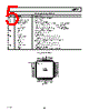
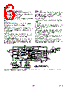
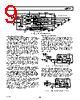
6 / 27 page  REV. B AD9767 –6– DEFINITIONS OF SPECIFICATIONS Linearity Error (Also Called Integral Nonlinearity or INL) Linearity error is defined as the maximum deviation of the actual analog output from the ideal output, determined by a straight line drawn from zero to full scale. Differential Nonlinearity (or DNL) DNL is the measure of the variation in analog value, normalized to full scale, associated with a 1 LSB change in digital input code. Monotonicity A D/A converter is monotonic if the output either increases or remains constant as the digital input increases. Offset Error The deviation of the output current from the ideal of zero is called offset error. For IOUTA, 0 mA output is expected when the inputs are all 0s. For IOUTB, 0 mA output is expected when all inputs are set to 1s. Gain Error The difference between the actual and ideal output span. The actual span is determined by the output when all inputs are set to 1s minus the output when all inputs are set to 0s. Output Compliance Range The range of allowable voltage at the output of a current-output DAC. Operation beyond the maximum compliance limits may cause either output stage saturation or breakdown resulting in nonlinear performance. Temperature Drift Temperature drift is specified as the maximum change from the ambient (+25 °C) value to the value at either TMIN or TMAX. For offset and gain drift, the drift is reported in ppm of full-scale range (FSR) per degree C. For reference drift, the drift is reported in ppm per degree C (ppm/ °C). Power Supply Rejection The maximum change in the full-scale output as the supplies are varied from nominal to minimum and maximum specified voltages. Settling Time The time required for the output to reach and remain within a specified error band about its final value, measured from the start of the output transition. Glitch Impulse Asymmetrical switching times in a DAC give rise to undesired output transients that are quantified by a glitch impulse. It is specified as the net area of the glitch in pV-s. Spurious-Free Dynamic Range The difference, in dB, between the rms amplitude of the output signal and the peak spurious signal over the specified bandwidth. Total Harmonic Distortion THD is the ratio of the rms sum of the first six harmonic components to the rms value of the measured input signal. It is expressed as a percentage or in decibels (dB). IOUTA2 IOUTB2 5V 50 IOUTA1 IOUTB1 SEGMENTED SWITCHES FOR DAC1 LSB SWITCH SEGMENTED SWITCHES FOR DAC2 LSB SWITCH DAC 2 LATCH DAC 1 LATCH CLK DIVIDER PMOS CURRENT SOURCE ARRAY PMOS CURRENT SOURCE ARRAY CLK1/IQCLK CLK2/IQRESET AVDD FSADJ1 REFIO FSADJ2 1.2V REF MODE DVDD MULTIPLEXING LOGIC 5V WRT2/ IQSEL WRT1/ IQWRT GAINCTRL 0.1 F RSET2 2k RSET1 2k 50 50 MINI CIRCUITS T1-1T TO HP3589A SPECTRUM/ NETWORK ANALYZER DCOM SLEEP ACOM DB0 – DB13 DB0 – DB13 DIGITAL DATA LECROY 9210 PULSE GENERATOR *RETIMED CLOCK OUTPUT DVDD DCOM AD9767 *AWG2021 CLOCK RETIMED SUCH THAT DIGITAL DATA TRANSITIONS ON FALLING EDGE OF 50% DUTY CYCLE CLOCK CHANNEL 2 LATCH CHANNEL 1 LATCH TEKTRONIX AWG-2021 w/OPTION 4 Figure 2. Basic AC Characterization Test Setup for AD9767, Testing Port 1 in Dual Port Mode, Using Independent GAINCTRL Resistors on FSADJ1 and FSADJ2 |
|
Ligação URL |
| ALLDATASHEET é útil para você? [ DONATE ] |
Sobre Alldatasheet | Publicidade | Contato conosco | Privacy Policy | Link para a ficha técnica | roca de Link | Lista de Fabricantes All Rights Reserved©Alldatasheet.com |
| Russian : Alldatasheetru.com | Korean : Alldatasheet.co.kr | Spanish : Alldatasheet.es | French : Alldatasheet.fr | Italian : Alldatasheetit.com Portuguese : Alldatasheetpt.com | Polish : Alldatasheet.pl | Vietnamese : Alldatasheet.vn Indian : Alldatasheet.in | Mexican : Alldatasheet.com.mx | British : Alldatasheet.co.uk | New Zealand : Alldatasheet.co.nz |
|
Family Site : ic2ic.com |
icmetro.com |
 Portuguese ▼
 English
 Chinese
 German
 Japanese
 Russian
 Korean
 Spanish
 French
 Italian
 Portuguese
 Polish
 Vietnamese
 Indian
 Mexican
 British
 New Zealand