|
Os motores de busca de Datasheet de Componentes eletrônicos |
|
|
Os motores de busca de Datasheet de Componentes eletrônicos |
|
LTC3602 Folha de dados(PDF) 8 Page - Linear Technology |
|
|
|||||||||||||||||||||||||||||
LTC3602 Folha de dados(HTML) 8 Page - Linear Technology |
|
|
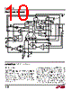
8 / 36 page  LTC3613 8 3613fa PIN FUNCTIONS PVIN (Pins 1-9, 53-56, 57 Exposed Pad): Power Supply Inputs. These pins connect to the drain of the internal power MOSFETS. The PVIN exposed pad must be soldered to the circuit board for electrical contact and rated thermal performance. The supply voltage can range from 4.5V to 24V. The voltage on this pin is also used to adjust the TG on-time in order to maintain constant frequency operation. SW (Pins 10, 35, 45-51, 58 Exposed Pad): Switch Node Connection. The (–) terminal of the bootstrap capacitor, CB, connects to this node. This pin swings from a diode voltage below ground up to VIN. The SW exposed pad must be soldered to the circuit board for electrical contact and rated thermal performance. BOOST (Pin 11): Boosted Driver Supply Connection. The (+) terminal of the bootstrap capacitor, CB, as well as the cathode of the Schottky diode, DB, connects to this node. This node swings from INTVCC – VSCHOTTKY to VIN + INTVCC – VSCHOTTKY. SGND (Pins 12, 16, 17, 19, 28, 29, 59 Exposed Pad): Signal Ground Connection. The SGND exposed pad must be soldered to the circuit board for electrical contact and rated thermal performance. All small-signal components should be connected to the signal ground. Connect signal ground to power ground only at one point using a single PCB trace. PGOOD (Pin 13): Power Good Indicator Output. This open-drain logic output is pulled to ground when the output voltage is outside of a ±7.5% window around the regulation point. SENSE+ (Pin 14): Differential Current Sensing (+) Input. For RSENSE current sensing, Kelvin (4-wire) connect SENSE+ and SENSE– pins across the sense resistor. For DCR sensing, Kelvin connect SENSE+ and SENSE– pins across the sense filter capacitor. SENSE– (Pin 15): Differential Current Sensing (–) Input. For RSENSE current sensing, Kelvin (4-wire) connect the SENSE+ and SENSE– pins across the sense resistor. For DCR sensing, Kelvin connect the SENSE+ and SENSE– pins across the sense filter capacitor. VOUT (Pin 18): Output voltage sense for adjusting the on-time for constant frequency operation. Tying this pin to the local output (instead of the remote output) is recom- mended for most applications. This pin can be programmed as needed for achieving the steady-state on-time required for constant frequency operation. VOSNS– (Pin 20): Differential Output Sensing (–) Input. Connect this pin to the negative terminal of the output capacitor. There is a bias current of 35μA (typical) flowing out of this pin. VOSNS+ (Pin 21): Differential Output Sensing (+) Input. Connect this pin to the feedback resistor divider between the positive and negative output capacitor terminals. In normal operation the LTC3613 will regulate the differen- tial output voltage which is divided down to 0.6V by the feedback resistor divider. TRACK/SS (Pin 22): External Tracking and Soft-Start Input. The LTC3613 regulates the differential feedback voltage (VOSNS+ − VOSNS–) to the smaller of 0.6V or the voltage on the TRACK/SS pin. An internal 1.0μA pull-up current source is connected to this pin. A capacitor to ground at this pin sets the ramp time to the final regulated output voltage. Alternatively, another voltage supply connected through a resistor divider to this pin allows the output to track the other supply during start-up. ITH (Pin 23): Current Control Voltage and Switching Regu- lator Compensation Point. The current sense threshold increases with this control voltage which ranges from 0V to 2.4V. VRNG (Pin 24): Current Sense Voltage Range Input. The maximum allowed sense voltage between SENSE+ and SENSE– is equal to 0.05 • VRNG. If VRNG is tied to SGND, the device operates with a maximum sense voltage of 30mV. If VRNG is tied to INTVCC, the device operates with a maximum sense voltage of 50mV. RT (Pin 25): Switching Frequency Programming Pin. Connect an external resistor from RT to signal ground to program the switching frequency between 200kHz and 1MHz. An external clock applied to MODE/PLLIN must be within ±30% of this free-running frequency to ensure frequency lock. |
|
Ligação URL |
| ALLDATASHEET é útil para você? [ DONATE ] |
Sobre Alldatasheet | Publicidade | Contato conosco | Privacy Policy | Link para a ficha técnica | roca de Link | Lista de Fabricantes All Rights Reserved©Alldatasheet.com |
| Russian : Alldatasheetru.com | Korean : Alldatasheet.co.kr | Spanish : Alldatasheet.es | French : Alldatasheet.fr | Italian : Alldatasheetit.com Portuguese : Alldatasheetpt.com | Polish : Alldatasheet.pl | Vietnamese : Alldatasheet.vn Indian : Alldatasheet.in | Mexican : Alldatasheet.com.mx | British : Alldatasheet.co.uk | New Zealand : Alldatasheet.co.nz |
|
Family Site : ic2ic.com |
icmetro.com |
 Portuguese ▼
 English
 Chinese
 German
 Japanese
 Russian
 Korean
 Spanish
 French
 Italian
 Portuguese
 Polish
 Vietnamese
 Indian
 Mexican
 British
 New Zealand