|
Os motores de busca de Datasheet de Componentes eletrônicos |
|
|
Os motores de busca de Datasheet de Componentes eletrônicos |
|
MAX16909 Folha de dados(PDF) 16 Page - Maxim Integrated Products |
|
|
|||||||||||||||||||||||||||||
MAX16909 Folha de dados(HTML) 16 Page - Maxim Integrated Products |
|
|
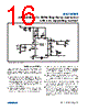
16 / 18 page  ���������������������������������������������������������������� Maxim Integrated Products 16 MAX16909 36V, 220kHz to 1MHz Step-Down Converter with Low Operating Current PCB Layout Guidelines Careful PCB layout is critical to achieve low switching losses and clean, stable operation. Use a multilayer board whenever possible for better noise immunity and power dissipation. Follow these guidelines for good PCB layout: 1) Use a large contiguous copper plane under the IC package. Ensure that all heat-dissipating components have adequate cooling. The bottom pad of the device must be soldered down to this copper plane for effec- tive heat dissipation and for getting the full power out of the IC. Use multiple vias or a single large via in this plane for heat dissipation. 2) Isolate the power components and high-current path from the sensitive analog circuitry. This is essential to prevent any noise coupling into the analog signals. 3) Keep the high-current paths short, especially at the ground terminals. This practice is essential for stable, jitter-free operation. The high-current path composed of input capacitor, high-side FET, inductor, and output capacitor should be as short as possible. 4) Keep the power traces and load connections short. This practice is essential for high efficiency. Use thick copper PCBs (2oz vs. 1oz) to enhance full-load efficiency. 5) The analog signal lines should be routed away from the high-frequency planes. This ensures integrity of sensitive signals feeding back into the IC. 6) The ground connection for the analog and power section should be close to the IC. This keeps the ground current loops to a minimum. In cases where only one ground is used, enough isolation between analog return signals and high-power signals must be maintained. Figure 4. 1.8V/3A Configuration D1 COUT 100µF C2 4.7µF C5 0.1µF RCOMP 9.1kI RPGOOD 10kI RFOSC 62kI L1 15µH VOUT 1.8V AT 3A CBST 0.1µF LX BST VOUT OUT VBAT FB VBIAS PGOOD FOSC CBIAS 1µF CCOMP2 12pF BIAS CCOMP1 821pF COMP FSYNC EN SUPSW SUP GND C1 47µF C4 0.1µF C3 4.7µF POWER GOOD MAX16909 R1 80.6kI R2 100kI |
|
|
Ligação URL |
| ALLDATASHEET é útil para você? [ DONATE ] |
Sobre Alldatasheet | Publicidade | Contato conosco | Privacy Policy | Link para a ficha técnica | roca de Link | Lista de Fabricantes All Rights Reserved©Alldatasheet.com |
| Russian : Alldatasheetru.com | Korean : Alldatasheet.co.kr | Spanish : Alldatasheet.es | French : Alldatasheet.fr | Italian : Alldatasheetit.com Portuguese : Alldatasheetpt.com | Polish : Alldatasheet.pl | Vietnamese : Alldatasheet.vn Indian : Alldatasheet.in | Mexican : Alldatasheet.com.mx | British : Alldatasheet.co.uk | New Zealand : Alldatasheet.co.nz |
|
Family Site : ic2ic.com |
icmetro.com |
 Portuguese ▼
 English
 Chinese
 German
 Japanese
 Russian
 Korean
 Spanish
 French
 Italian
 Portuguese
 Polish
 Vietnamese
 Indian
 Mexican
 British
 New Zealand