|
Os motores de busca de Datasheet de Componentes eletrônicos |
|
|
Os motores de busca de Datasheet de Componentes eletrônicos |
|
MAX16909 Folha de dados(PDF) 11 Page - Maxim Integrated Products |
|
|
|||||||||||||||||||||||||||||
MAX16909 Folha de dados(HTML) 11 Page - Maxim Integrated Products |
|
|
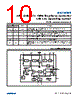
11 / 18 page  ���������������������������������������������������������������� Maxim Integrated Products 11 MAX16909 36V, 220kHz to 1MHz Step-Down Converter with Low Operating Current Detailed Description The MAX16909 is a constant-frequency, current-mode, automotive buck converter with an integrated high-side switch. The device operates with input voltages from 3.5V to 36V and tolerates input transients from 3.5V up to 42V. During undervoltage events, such as cold-crank condi- tions, the internal pass device maintains 98% duty cycle. The switching frequency is resistor programmable from 220kHz to 1MHz to allow optimization for efficiency, noise, and board space. A synchronization input FSYNC allows the device to synchronize to an external clock frequency. During light-load conditions, the device enters skip mode for high efficiency. The 5V fixed output voltage eliminates the need for external resistors and reduces the supply current to 30FA. See the Internal Block Diagram for more information. Wide Input Voltage Range (3.5V to 36V) The device includes two separate supply inputs, SUP and SUPSW, specified for a wide 3.5V to 36V input voltage range. VSUP provides power to the device and VSUPSW provides power to the internal switch. When the device is operating with a 3.5V input supply, certain conditions such as cold crank can cause the voltage at SUPSW to drop below the programmed output voltage. As such, the device operates in a high duty-cycle mode to maintain output regulation. Linear Regulator Output (BIAS) The device includes a 5V linear regulator, BIAS, that provides power to the internal circuitry. Connect a 1FF ceramic capacitor from BIAS to GND. External Clock Input (FSYNC) The device synchronizes to an external clock signal applied at FSYNC. The signal at FSYNC must have a 10% higher frequency than the internal clock frequency for proper synchronization. Soft-Start The device includes an 8.5ms fixed soft-start time for up to 500FF capacitive load with a 3A resistive load. Minimum On-Time The device features a 80ns minimum on-time that ensures proper operation at 1MHz switching frequency and high differential voltage between the input and the output. This feature is extremely beneficial in automo- tive applications where the board space is limited and the converter needs to maintain a well-regulated output voltage using an input voltage that varies from 9V to 18V. Additionally, the device incorporates an innovative design for fast-loop response that further ensures good output-voltage regulation during transients. System Enable (EN) An enable-control input (EN) activates the device from its low-power shutdown mode. EN is compatible with inputs from automotive battery level down to 3.3V. The high- voltage compatibility allows EN to be connected to SUP, KEY/KL30, or the INH pin of a CAN transceiver. EN turns on the internal regulator. Once VBIAS is above the internal lockout threshold, VUVL = 3.15V (typ), the controller activates and the output voltage ramps up within 8.5ms. A logic-low at EN shuts down the device. During shut- down, the internal linear regulator and gate drivers turn off. Shutdown is the lowest power state and reduces the quiescent current to 5FA (typ). Drive EN high to bring the device out of shutdown. Overvoltage Protection The device includes overvoltage protection circuitry that protects the device when there is an overvoltage condi- tion at the output. If the output voltage increases by more than 110% of its set voltage, the device stops switching. The device resumes regulation once the overvoltage condition is removed. Fast Load-Transient Response Current-mode buck converters include an integrator architecture and a load-line architecture. The integra- tor architecture has large loop gain but slow transient response. The load-line architecture has fast transient response but low loop gain. The device features an inte- grator architecture with innovative designs to improve transient response. Thus, the device delivers high output- voltage accuracy, plus the output can recover quickly from a transient overshoot, which could damage other on-board components during load transients. Overload Protection The overload protection circuitry is triggered when the device is in current limit and VOUT is below the reset threshold. Under these conditions the device turns the high-side FET off for 16ms and re-enters soft-start. If the overload condition is still present, the device repeats the cycle. |
|
|
Ligação URL |
| ALLDATASHEET é útil para você? [ DONATE ] |
Sobre Alldatasheet | Publicidade | Contato conosco | Privacy Policy | Link para a ficha técnica | roca de Link | Lista de Fabricantes All Rights Reserved©Alldatasheet.com |
| Russian : Alldatasheetru.com | Korean : Alldatasheet.co.kr | Spanish : Alldatasheet.es | French : Alldatasheet.fr | Italian : Alldatasheetit.com Portuguese : Alldatasheetpt.com | Polish : Alldatasheet.pl | Vietnamese : Alldatasheet.vn Indian : Alldatasheet.in | Mexican : Alldatasheet.com.mx | British : Alldatasheet.co.uk | New Zealand : Alldatasheet.co.nz |
|
Family Site : ic2ic.com |
icmetro.com |
 Portuguese ▼
 English
 Chinese
 German
 Japanese
 Russian
 Korean
 Spanish
 French
 Italian
 Portuguese
 Polish
 Vietnamese
 Indian
 Mexican
 British
 New Zealand