|
Os motores de busca de Datasheet de Componentes eletrônicos |
|
|
Os motores de busca de Datasheet de Componentes eletrônicos |
|
CLC2058 Folha de dados(PDF) 9 Page - Cadeka Microcircuits LLC. |
|
|
|||||||||||||||||||||||||||||
CLC2058 Folha de dados(HTML) 9 Page - Cadeka Microcircuits LLC. |
|
|
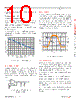
9 / 12 page  Data Sheet ©2007-2009 CADEKA Microcircuits LLC www.cadeka.com 9 Application Information Basic Operation Figures 1, 2, and 3 illustrate typical circuit configurations for non-inverting, inverting, and unity gain topologies for dual supply applications. They show the recommended bypass capacitor values and overall closed loop gain equations. + - Rf 0.1μF 6.8μF Output G = 1 + (Rf/Rg) Input +Vs -Vs Rg 0.1μF 6.8μF RL Figure 1. Typical Non-Inverting Gain Circuit Figure 2. Typical Inverting Gain Circuit + - 0.1μF 6.8μF Output G = 1 Input +Vs -Vs 0.1μF 6.8μF RL Figure 3. Unity Gain Circuit Power Dissipation Power dissipation should not be a factor when operating under the stated 2k ohm load condition. However, ap- plications with low impedance, DC coupled loads should be analyzed to ensure that maximum allowed junction temperature is not exceeded. Guidelines listed below can be used to verify that the particular application will not cause the device to operate beyond it’s intended operat- ing range. Maximum power levels are set by the absolute maximum junction rating of 150°C. To calculate the junction tem- perature, the package thermal resistance value ThetaJA (ӨJA) is used along with the total die power dissipation. TJunction = TAmbient + (ӨJA × PD) Where TAmbient is the temperature of the working environment. In order to determine PD, the power dissipated in the load needs to be subtracted from the total power delivered by the supplies. PD = Psupply - Pload Supply power is calculated by the standard power equa- tion. Psupply = Vsupply × IRMS supply Vsupply = VS+ - VS- Power delivered to a purely resistive load is: Pload = ((VLOAD)RMS2)/Rloadeff The effective load resistor (Rloadeff) will need to include the effect of the feedback network. For instance, Rloadeff in figure 3 would be calculated as: RL || (Rf + Rg) These measurements are basic and are relatively easy to perform with standard lab equipment. For design purpos- es however, prior knowledge of actual signal levels and load impedance is needed to determine the dissipated power. Here, PD can be found from PD = PQuiescent + PDynamic - PLoad Quiescent power can be derived from the specified IS val- ues along with known supply voltage, VSupply. Load power + - Rf 0.1μF 6.8μF Output G = - (Rf/Rg) For optimum input offset voltage set R1 = Rf || Rg Input +Vs -Vs 0.1μF 6.8μF RL Rg R1 |
|
|
Ligação URL |
| ALLDATASHEET é útil para você? [ DONATE ] |
Sobre Alldatasheet | Publicidade | Contato conosco | Privacy Policy | Link para a ficha técnica | roca de Link | Lista de Fabricantes All Rights Reserved©Alldatasheet.com |
| Russian : Alldatasheetru.com | Korean : Alldatasheet.co.kr | Spanish : Alldatasheet.es | French : Alldatasheet.fr | Italian : Alldatasheetit.com Portuguese : Alldatasheetpt.com | Polish : Alldatasheet.pl | Vietnamese : Alldatasheet.vn Indian : Alldatasheet.in | Mexican : Alldatasheet.com.mx | British : Alldatasheet.co.uk | New Zealand : Alldatasheet.co.nz |
|
Family Site : ic2ic.com |
icmetro.com |
 Portuguese ▼
 English
 Chinese
 German
 Japanese
 Russian
 Korean
 Spanish
 French
 Italian
 Portuguese
 Polish
 Vietnamese
 Indian
 Mexican
 British
 New Zealand