|
Os motores de busca de Datasheet de Componentes eletrônicos |
|
|
Os motores de busca de Datasheet de Componentes eletrônicos |
|
LTC1749 Folha de dados(PDF) 1 Page - Linear Technology |
|
|
|||||||||||||||||||||||||||||
LTC1749 Folha de dados(HTML) 1 Page - Linear Technology |
|
|
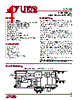
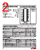
1 / 20 page  1 LTC1749 1749f 12-Bit, 80Msps Wide Bandwidth ADC s Sample Rate: 80Msps s PGA Front End (2.25VP-P or 1.35VP-P Input Range) s 71.8dB SNR and 87dB SFDR (PGA = 0) s 70.2dB SNR and 87dB SFDR (PGA = 1) s 500MHz Full Power Bandwidth S/H s No Missing Codes s Single 5V Supply s Power Dissipation: 1.45W s Two Pin Selectable Reference Values s Data Ready Output Clock s Pin Compatible 14-Bit 80Msps Device (LTC1750) s 48-Pin TSSOP Package s Direct IF Sampling s Telecommunications s Receivers s Cellular Base Stations s Spectrum Analysis s Communications Test Equipment s Undersampling , LTC and LT are registered trademarks of Linear Technology Corporation. The LTC ®1749 is an 80Msps, 12-bit A/D converter de- signed for digitizing wide dynamic range signals up to frequencies of 500MHz. The input range of the ADC can be optimized with the on-chip PGA sample-and-hold circuit and flexible reference circuitry. The LTC1749 has a highly linear sample-and-hold circuit with a bandwidth of 500MHz. The SFDR is 80dB with an input frequency of 250MHz. Ultralow jitter of 0.15psRMS allows undersampling of IF frequencies with minimal degradation in SNR. DC specs include ±1LSB INL and no missing codes. The digital interface is compatible with 5V, 3V, 2V and LVDS logic systems. The ENC and ENC inputs may be driven differentially from PECL, GTL and other low swing logic families or from single-ended TTL or CMOS. The low noise, high gain ENC and ENC inputs may also be driven by a sinusoidal signal without degrading performance. A separate output power supply can be operated from 0.5V to 5V, making it easy to connect directly to low voltage DSPs or FIFOs. The 48-pin TSSOP package with a flow-through pinout simplifies the board layout. 80Msps, 12-Bit ADC with a 2.25V Differential Input Range DESCRIPTIO FEATURES APPLICATIO S BLOCK DIAGRA 12-BIT PIPELINED ADC 12 S/H CIRCUIT ±1.125V DIFFERENTIAL ANALOG INPUT AIN + PGA AIN – SENSE VCM 4.7 µF DIFF AMP REFLA REFHB GND 1749 BD ENC 4.7 µF 1 µF1µF 0.1 µF 0.1 µF REFHA REFLB BUFFER RANGE SELECT 2VREF CORRECTION LOGIC AND SHIFT REGISTER OUTPUT LATCHES CONTROL LOGIC OVDD VDD OGND 0.5V TO 5V 5V 0.1 µF 1 µF 1 µF 1 µF D11 D0 CLKOUT • • • ENC DIFFERENTIAL ENCODE INPUT MSBINV 0.1 µF |
Nº de peça semelhante - LTC1749 |
|
Descrição semelhante - LTC1749 |
|
|
|
Ligação URL |
| ALLDATASHEET é útil para você? [ DONATE ] |
Sobre Alldatasheet | Publicidade | Contato conosco | Privacy Policy | Link para a ficha técnica | roca de Link | Lista de Fabricantes All Rights Reserved©Alldatasheet.com |
| Russian : Alldatasheetru.com | Korean : Alldatasheet.co.kr | Spanish : Alldatasheet.es | French : Alldatasheet.fr | Italian : Alldatasheetit.com Portuguese : Alldatasheetpt.com | Polish : Alldatasheet.pl | Vietnamese : Alldatasheet.vn Indian : Alldatasheet.in | Mexican : Alldatasheet.com.mx | British : Alldatasheet.co.uk | New Zealand : Alldatasheet.co.nz |
|
Family Site : ic2ic.com |
icmetro.com |
 Portuguese ▼
 English
 Chinese
 German
 Japanese
 Russian
 Korean
 Spanish
 French
 Italian
 Portuguese
 Polish
 Vietnamese
 Indian
 Mexican
 British
 New Zealand