22 / 22 page

22 of 22
RF2498
Rev A3 DS030711
7628 Thorndike Road, Greensboro, NC 27409-9421 · For sales or technical
support, contact RFMD at (+1) 336-678-5570 or sales-support@rfmd.com.
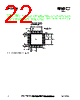
PCB Solder Mask Pattern
Liquid Photo-Imageable (LPI) solder mask is recommended. The solder mask footprint will match what is shown for the PCB
metal land pattern with a 2mil to 3mil expansion to accommodate solder mask registration clearance around all pads. The
center-grounding pad shall also have a solder mask clearance. Expansion of the pads to create solder mask clearance can be
provided in the master data or requested from the PCB fabrication supplier.
A
A
A
A
A
A
A
A
B B B B B B B B
A
A
A
A
A
A
A
A
B
B
B
B
B
B
B
B
C
3.50 Typ.
0.50 Typ.
0.50 Typ.
0.55 Typ.
1.75 Typ.
1.75 Typ.
0.55 Typ.
3.50 Typ.
A = 0.74 x 0.38 (mm) Typ.
B = 0.38 x 0.74 (mm) Typ.
C = 3.60 (mm) Sq.
Pin 1
Pin 32
Pin 24
Pin 16
Dimensions in mm.
Figure 2. PCB Solder Mask Pattern (Top View)


 Portuguese ▼
 English
 Chinese
 German
 Japanese
 Russian
 Korean
 Spanish
 French
 Italian
 Portuguese
 Polish
 Vietnamese
 Indian
 Mexican
 British
 New Zealand