14 of 22
RF2498
Rev A3 DS030711
7628 Thorndike Road, Greensboro, NC 27409-9421 · For sales or technical
support, contact RFMD at (+1) 336-678-5570 or sales-support@rfmd.com.
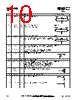
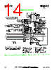
Application Schematic
NOTE: IF output matching component values are dependent on board layout, IF SAW filter and the IF frequency selected.
Please contact RFMD application engineering for assistance with IF output matching.
TBD
7.5 k
Ω
TBD
TBD
TBD
TBD
TBD
TBD
TBD
TBD
MIX GAIN
ENABLE
2.4 pF
33 nF
LNA GAIN
33 nF
18 nH
6.8 nH
33 nF
20 k
Ω
5.1 k
Ω
TBD
32
1
9
17
2
3
4
5
6
7
8
10
11
12
13
14
15
16
24
23
22
21
20
19
18
31
30
29
28
27
26
25
TBD
TBD
4
5
10
9
CDMA
IF SAW
TBD
TBD
TBD
TBD
TBD
4
5
10
9
FM
IF SAW
2.2 nH
DIV EN
TX BUF EN
3.3 nH
1.0 pF
33 nF
IP SET
1.2 nH
10 nH
Cell
RF Saw
6
3
4
1
GND
GND
GND
GND
33 nF
1 pF
PCS
RF Saw
GND
GND
GND
GND
6
3
4
1
33 nF
33 nH
4.7 nH
2.7 nH
10
Ω
IF SEL
BAND SEL
V
CC
V
CC
V
CC
V
CC
V
CC
V
CC
V
CC
GPS IF
V
CC
LO IN
LO OUT
V
CC
CELL LNA IN
PCS LNA IN
GPS LNA IN
FM+
FM-
200
Ω
CDMA+
CDMA-
NOTES:
1. This resistor sets mixer preamp and mixer currents in all bands.
Lowering the resistance results in higher currents.
2. This resistor sets LNA currents of all bands in boost mode.
Increasing the resistor value results in lower currents.
3. Sets internal bias voltage. Recommend 5.1 k
Ω.
4. DC blocking capacitor.
5. PCS LNA Input Matching. Optimize for NF.
6. Determines trade off between IIP3 and Gain.
Higher value inductor means lower gain and higher IIP3.
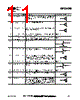
7. Cell/PCS LNA Input Matching for optimum IIP3.
Low impedance path to ground at low frequency for optimum IIP3.
8. For cell and PCS mixer input matching.
Note: If any functional blocks are not being used, the unused pins can be left with no connection.
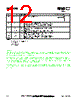
Layout Note:
To minimize losses and radiation, the RF signal traces should be as short as possible. The IF+ and
IF- outputs traces should be symmetrical. All bypass capacitors and matching capacitors must
have a ground via very close to the capacitor. Each capacitor should have its own ground via. All
traces should be 50
Ω transmission lines. Position inductors to reduce coupling (see note 15).
9. PCS Interstage matching. As the value of the inductance is increased,
the PCS mixer preamp gain will decrease and the IIP3 will increase
and vice versa.
10. For optimum NF and input matching. As the value of the capacitance
is increased, the NF will become worse.
11. To optimize performance over temperature and bias.
12. For output matching and a DC supply bias choke.
13. GPS mixer input matching for optimum IIP3.
Low impedance path to ground at low frequency for optimum IIP3.
14. Input or Output matching.
15. Coupling of coils on the input, output, and emitter (where applicable)
of any LNA should be minimized to reduce the risk of oscillation. We
recommend separating the inductors and/or positioning them 90o
relative to each other.
33 nH
1.2 pF
2.7 nH
33 nF
33 nH
1.2 nH
0.75 pF
15
Ω
TBD
V
CC
TBD
GPS
RF Saw
52
OUT
IN
See Notes
12 and 15
See Notes
6 and 15
See
Notes
7 and 15
See Note 4
See Notes
14 and 15
See Notes
12 and 15
See Note 11
See Note 14
See
Note 11
See
Note 2
See Note 3
See Note 1
See Note 9
See Note 8
See Note 4
See Note 4
See Note 14
See Note 8
See Note 4
See
Note 14
See
Note 10
See Note 4
See Notes
14 and 15
See Note 4
See Notes
14 and 15
See
Note 10
See Notes
7 and 15
See Notes
12 and 15
See Note 13
See
Note 4


 Portuguese ▼
 English
 Chinese
 German
 Japanese
 Russian
 Korean
 Spanish
 French
 Italian
 Portuguese
 Polish
 Vietnamese
 Indian
 Mexican
 British
 New Zealand