|
Os motores de busca de Datasheet de Componentes eletrônicos |
|
|
Os motores de busca de Datasheet de Componentes eletrônicos |
|
TC7109CLW Folha de dados(PDF) 15 Page - Microchip Technology |
|
|
|||||||||||||||||||||||||||||
TC7109CLW Folha de dados(HTML) 15 Page - Microchip Technology |
|
|
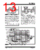
15 / 30 page  © 2006 Microchip Technology Inc. DS21456C-page 15 TC7109/A 3.4 Test Input The counter and its outputs may be tested easily. When the TEST input is connected to GND, the internal clock is disabled and the counter outputs are all forced into the HIGH state. When the input returns to the 1/2 (V+ – GND) voltage or to V+ and one clock is input, the counter outputs will all be clocked to the LOW state. The counter output latches are enabled when the TEST input is taken to a level halfway between V+ and GND, allowing the counter contents to be examined any time. 3.5 Component Value Selection The integrator output swing for full scale should be as large as possible. For example, with ±5V supplies and COMMON connected to GND, the nominal integrator output swing at full scale is ±4V. Since the integrator output can go to 0.3V from either supply without signif- icantly effecting linearity, a 4V integrator output swing allows 0.7V for variations in output swing, due to com- ponent value and oscillator tolerances. With ±5V sup- plies and a Common mode voltage range of ±1V required, the component values should be selected to provide ±3V integrator output swing. Noise and roll- over errors will be slightly worse than in the ±4V case. For large Common mode voltage ranges, the integrator output swing must be reduced further. This will increase both noise and rollover errors. To improve performance, ±6V supplies may be used. 3.5.1 INTEGRATING CAPACITOR The integrating capacitor, CINT, should be selected to give the maximum integrator output voltage swing that will not saturate the integrator to within 0.3V from either supply. A ±3.5V to ±4V integrator output swing is nom- inal for the TC7109A, with ±5V supplies and analog common connected to GND. For 7-1/2 conversions per second (61.72kHz internal clock frequency), nominal values CINT and CAZ are 0.15μF and 0.33μF, respec- tively. These values should be changed if different clock frequencies are used to maintain the integrator output voltage swing. The value of CINT is given by: EQUATION 3-2: The integrating capacitor must have low dielectric absorption to prevent rollover errors. Polypropylene capacitors give undetectable errors, at reasonable cost, up to +85°C. 3.5.2 INTEGRATING RESISTOR The integrator and buffer amplifiers have a class A out- put stage with 100 μA of quiescent current. They supply 20 μA of drive current with negligible non-linearity. The integrating resistor should be large enough to remain in this very linear region over the input voltage range, but small enough that undue leakage requirements are not placed on the PC board. For 2.048V full scale, a 100k Ω resistor is recommended and for 409.6mV full scale, a 20k resistor is recommended. RINT may be selected for other values of full scale by: EQUATION 3-3: 3.5.3 AUTO-ZERO CAPACITOR As the auto-zero capacitor is made large, the system noise is reduced. Since the TC7109A incorporates a zero integrator cycle, the size of the auto-zero capaci- tor does not affect overload recovery. The optimal value of the auto-zero capacitor is between 2 and 4 times CINT. A typical value for CAZ is 0.33μF. The inner foil of CAZ should be connected to Pin 31 and the outer foil to the RC summing junction. The inner foil of CINT should be connected to the RC summing junction and the outer foil to Pin 32, for best rejection of stray pickups. 3.5.4 REFERENCE CAPACITOR A 1 μF capacitor is recommended for most circuits. However, where a large Common mode voltage exists, a larger value is required to prevent rollover error (e.g., the reference low is not analog common), and a 409.6mV scale is used. The rollover error will be held to 0.5 count with a 10 μF capacitor. 3.5.5 REFERENCE VOLTAGE To generate full scale output of 4096 counts, the analog input required is VIN = 2VREF. For 409.6mV full scale, use a reference of 204.8mV. In many applications, where the ADC is connected to a transducer, a scale factor will exist between the input voltage and the digital reading. For instance, in a measuring system, the designer might like to have a full scale reading when the voltage for the transducer is 700mV. Instead of dividing the input down to 409.6mV, the designer should use the input voltage directly and select VREF = 350mV. Suitable values for integrating resistor and capacitor would be 34k Ω and 0.15μF. This makes the system slightly quieter and also avoids a divider network on the input. Another advantage of this system occurs when temperature and weight measurements, with an offset or tare, are desired for non-zero input. The offset may be introduced by connecting the voltage output of the transducer between common and analog high, and the offset voltage between common and ana- log low, observing polarities carefully. In processor based systems using the TC7109A, it may be more desirable to use software and perform this type of scaling or tare subtraction digitally. (2048 Clock Period) (20 μA) Integrator Output Voltage Swings CINT = Full Scale Voltage 20 μA RINT = |
|
Ligação URL |
| ALLDATASHEET é útil para você? [ DONATE ] |
Sobre Alldatasheet | Publicidade | Contato conosco | Privacy Policy | Link para a ficha técnica | roca de Link | Lista de Fabricantes All Rights Reserved©Alldatasheet.com |
| Russian : Alldatasheetru.com | Korean : Alldatasheet.co.kr | Spanish : Alldatasheet.es | French : Alldatasheet.fr | Italian : Alldatasheetit.com Portuguese : Alldatasheetpt.com | Polish : Alldatasheet.pl | Vietnamese : Alldatasheet.vn Indian : Alldatasheet.in | Mexican : Alldatasheet.com.mx | British : Alldatasheet.co.uk | New Zealand : Alldatasheet.co.nz |
|
Family Site : ic2ic.com |
icmetro.com |
 Portuguese ▼
 English
 Chinese
 German
 Japanese
 Russian
 Korean
 Spanish
 French
 Italian
 Portuguese
 Polish
 Vietnamese
 Indian
 Mexican
 British
 New Zealand