3 / 10 page

4-539
RF3220
Rev A1 050822
Pin
Function
Description
Interface Schematic
1GND
Ground connection.
2RF IN
RF input pin. This pin is not internally DC-blocked. A DC blocking
capacitor suitable for the frequency of operation should be used.
3GND
Ground connection.
4GND
Ground connection.
5GND
Ground connection.
6GND
Ground connection.
7GND
Ground connection.
8RF OUT
Amplifier output pin. This pin is an open-collector output. It must be
biased to VCC through a choke or matching inductor. This pin is typi-
cally matched to 50
Ω with a shunt bias/matching inductor and series
blocking/matching capacitor. Refer to application schematics.
See pin 2.
9GND
Ground connection.
10
GND
Ground connection.
11
BIAS
This pin is used to control the bias current. An external resistor may be
used to set the bias current for any VPD voltage. Allows for trade-offs
between IP3 versus noise figure and TMAX.
12
GND
Ground connection.
Pkg
Base
GND
Ground connection. Vias to ground required under the package base.
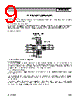
RF IN
RF OUT
To Bias
Circuit
V
CC


 Portuguese ▼
 English
 Chinese
 German
 Japanese
 Russian
 Korean
 Spanish
 French
 Italian
 Portuguese
 Polish
 Vietnamese
 Indian
 Mexican
 British
 New Zealand