|
Os motores de busca de Datasheet de Componentes eletrônicos |
|
|
Os motores de busca de Datasheet de Componentes eletrônicos |
|
LT6211CDD Folha de dados(PDF) 6 Page - Linear Technology |
|
|
|||||||||||||||||||||||||||||
LT6211CDD Folha de dados(HTML) 6 Page - Linear Technology |
|
|
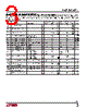
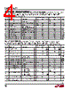
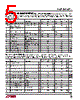
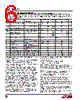
6 / 16 page  6 LT6210/LT6211 62101f SYMBOL PARAMETER CONDITIONS MIN TYP MAX MIN TYP MAX UNITS CMRR Common Mode Rejection Ratio VIN = V + – 1.2V to V– + 1.2V 46 50 46 dB q 43 dB –ICMRR Inverting Input Current VIN = V+ – 1.2V to V– + 1.2V 0.15 ±1.5 0.2 µA/V Common Mode Rejection q ±2 µA/V PSRR Power Supply Rejection Ratio VS = ±1.5V to ±6V (Note 6) q 60 85 60 85 dB –IPSRR Inverting Input Current VS = ±1.5V to ±6V (Note 6) 0.4 ±2.2 0.4 ±2.2 µA/V Power Supply Rejection q ±4 ±4 µA/V IS Supply Current per Amplifier 0.3 0.525 0.3 0.38 mA q 0.6 0.43 mA IOUT Maximum Output Current RL = 0Ω q ±30 ±10 mA (Notes 7, 11) ROL Transimpedance, ∆VOUT/∆IIN–VOUT = V+ – 1.2V to V– + 1.2V 300 660 65 120 k Ω SR Slew Rate (Note 8) 120 170 20 V/ µs tpd Propagation Delay 50% VIN to 50% VOUT,30 50 ns 100mVP-P, Larger of tpd+, tpd– BW –3dB Bandwidth <1dB Peaking, AV = 1 10 7.5 MHz ts Settling Time To 0.1% of VFINAL, VSTEP = 2V 200 300 ns tf, tr Small-Signal Rise and Fall Time 10% to 90%, VOUT = 100mVP-P 40 50 ns HD2 2nd Harmonic Distortion f = 1MHz, VOUT = 2VP-P –40 –45 dBc HD3 3rd Harmonic Distortion f = 1MHz, VOUT = 2VP-P –45 –45 dBc (IS = 300µA per Amplifier) The q denotes specifications which apply over the specified operating temperature range, otherwise specifications are at TA = 25°C. For V+ = 5V, V– = – 5V: RSET = 1M to ground, AV = +2, RF = RG = 11k, RL = 1k; For V+ = 3V, V– = 0V: RSET = 270k to V–, AV = +2, RF = 9.31k, RG = 9.31k to 1.5V, RL = 1k to 1.5V unless otherwise specified. V+ = 5V, V– = –5V, IS = 300µA V+ = 3V, V– = 0V, IS = 300µA ELECTRICAL CHARACTERISTICS Note 1: Absolute Maximum Ratings are those values beyond which the life of a device may be impaired. Note 2: As long as output current and junction temperature are kept below the absolute maximum ratings, no damage to the part will occur. Depending on the supply voltage, a heat sink may be required. Note 3: The LT6210C/LT6211C is guaranteed functional over the operating temperature range of –40 °C to 85°C. Note 4: The LT6210C/LT6211C is guaranteed to meet specified perfor- mance from 0 °C to 70°C. The LT6210C/LT6211C is designed, character- ized and expected to meet specified performance from –40 °C and 85°C but is not tested or QA sampled at these temperatures. The LT6210I/ LT6211I is guaranteed to meet specified performance from –40 °C to 85°C. Note 5: The LT6210 with no metal connected to the V– pin has a θJA of 230 °C/W, however, thermal resistances vary depending upon the amount of PC board metal attached to Pin 2 of the device. With the LT6210 mounted on a 2500mm2 3/32" FR-4 board covered with 2oz copper on both sides and with just 20mm2 of copper attached to Pin 2, θJA drops to 160 °C/W. Thermal performance can be improved even further by using a 4-layer board or by attaching more metal area to Pin 2. Thermal resistance of the LT6211 in MSOP-10 is specified for a 2500mm2 3/32" FR-4 board covered with 2oz copper on both sides and with 100mm2 of copper attached to Pin 5. Its performance can also be increased with additional copper much like the LT6210. To achieve the specified θJA of 43°C/W for the LT6211 DFN-10, the exposed pad must be soldered to the PCB. In this package, θJA will benefit from increased copper area attached to the exposed pad. TJ is calculated from the ambient temperature TA and the power dissipa- tion PD according to the following formula: TJ = TA + (PD • θJA) The maximum power dissipation can be calculated by: PD(MAX) = (VS • IS(MAX)) + (VS/2)2/RLOAD Note 6: For PSRR and –IPSRR testing, the current into the ISET pin is constant, maintaining a consistent LT6210/LT6211 quiescent bias point. A graph of PSRR vs Frequency is included in the Typical Performance Characteristics showing +PSRR and –PSRR with RSET connecting ISET to ground. Note 7: While the LT6210 and LT6211 circuitry is capable of significant output current even beyond the levels specified, sustained short-circuit current exceeding the Absolute Maximum Rating of ±80mA may permanently damage the device. Note 8: This parameter is guaranteed to meet specified performance through design and characterization. It is not production tested. Note 9: Differential gain and phase are measured using a Tektronix TSG120YC/NTSC signal generator and a Tektronix 1780R Video Measure- ment Set. The resolution of this equipment is 0.1% and 0.1 °. Five identical amplifier stages were cascaded giving an effective resolution of 0.02% and 0.02 °. Note 10: Input voltage range on ±5V dual supplies is guaranteed by CMRR. On 3V single supply it is guaranteed by design and by correlation to the ±5V input voltage range limits. Note 11: This parameter is tested by forcing a 50mV differential voltage between the inverting and noninverting inputs. |
|
|
Ligação URL |
| ALLDATASHEET é útil para você? [ DONATE ] |
Sobre Alldatasheet | Publicidade | Contato conosco | Privacy Policy | Link para a ficha técnica | roca de Link | Lista de Fabricantes All Rights Reserved©Alldatasheet.com |
| Russian : Alldatasheetru.com | Korean : Alldatasheet.co.kr | Spanish : Alldatasheet.es | French : Alldatasheet.fr | Italian : Alldatasheetit.com Portuguese : Alldatasheetpt.com | Polish : Alldatasheet.pl | Vietnamese : Alldatasheet.vn Indian : Alldatasheet.in | Mexican : Alldatasheet.com.mx | British : Alldatasheet.co.uk | New Zealand : Alldatasheet.co.nz |
|
Family Site : ic2ic.com |
icmetro.com |
 Portuguese ▼
 English
 Chinese
 German
 Japanese
 Russian
 Korean
 Spanish
 French
 Italian
 Portuguese
 Polish
 Vietnamese
 Indian
 Mexican
 British
 New Zealand