 |
Os motores de busca de Datasheet de Componentes eletrônicos |
|
|
Os motores de busca de Datasheet de Componentes eletrônicos |
|
The question interval is too short.
Please try again in a few seconds.

Hello, Please ask a question about RF2890 Datasheet
# Example questions:
➢ What is the typical size of the pcb metal land pattern (in mm) for the square pads?
➢ What is the primary purpose of the l2 and c3 components within the differential if matching network?
➢ What surface finish is recommended for the pcb used with this rf component?
| Part No. | RF2890 |
| Manufacturer | RFMD |
| Size | 183 Kbytes |
| Pages | 14 pages |
| Description | DUAL-BAND CDMA CELLULAR/GPS LOW NOISE AMPLIFIER/MIXER |


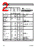


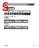

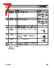

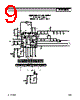


1. Core Functionality:
️· RF Transceiver: This IC is a complete RF transceiver solution, handling both transmitting and receiving of radio signals.
️· Frequency Bands: While not explicitly stated, the documentation heavily references IF frequencies (183.6 MHz) and references SAW filters, which implies operation in the sub-GHz range. It's likely intended for GSM, EDGE, UMTS, or perhaps newer sub-6GHz technologies.
️· Low Noise Amplifier (LNA): Includes a LNA for sensitive signal reception.
️· Mixer: Key component for frequency up/down conversion.
️· IF Filtering: Offers both SAW (Surface Acoustic Wave) and LC filtering options for the Intermediate Frequency.
️· Open Collector Outputs: Uses open-collector outputs, likely for flexibility in interfacing with external filters and amplifiers.
2. Key Features & Considerations:
️· Integrated Design: High level of integration minimizes external component count, reducing size and cost.
️· IF Filtering Options: Supports both SAW and LC filters, providing design flexibility based on performance requirements. SAW filters are generally better for selectivity and insertion loss, while LC filters can be more cost-effective.
️· Single-Ended and Differential IF Matching: Provides both single-ended and differential matching networks for the IF stage, allowing designers to optimize performance for their specific application.
️· Current Combiner: Uses current combiner techniques to optimize the IF output.
️· PCB Design Requirements: Strict PCB design guidelines are provided, especially regarding surface finish, land patterns, and grounding. This is crucial for achieving optimal RF performance.
️· Open Collector Outputs: Employs open-collector outputs, providing flexibility in interfacing with external filters and amplifiers.
3. Application Focus:
️· Cellular Handsets: A primary target application appears to be cellular phones (GSM, UMTS, etc.).
️· Wireless Data Devices: Could be used in other wireless data devices, such as modems, routers, or IoT devices.
4. Specific Technical Highlights:
️· IF Frequency: 183.6 MHz is the primary IF frequency referenced.
️· Matching Networks: Detailed instructions are given for designing IF matching networks, both single-ended and differential.
️· Filtering Options: SAW and LC filtering.
️· PCB Material: Electroless nickel immersion gold (ENIG) is preferred for the PCB surface finish.
5. Areas for Further Investigation (Based on the excerpt):
️· Complete Frequency Range: What is the complete supported frequency range of the IC?
️· Data Rates: What data rates can the IC support?
️· Power Consumption: What is the power consumption of the IC?
️· Digital Interface: How does the IC interface with a baseband processor or other digital circuitry?
In summary, this is a very detailed technical document describing a sophisticated RF transceiver IC. It's clearly targeted at experienced RF engineers who need a high-performance, integrated solution for wireless communication applications. The stringent PCB design requirements highlight the importance of careful layout and fabrication to achieve optimal performance.
1. Core Functionality:
️· RF Transceiver: This IC is a complete RF transceiver solution, handling both transmitting and receiving of radio signals.
️· Frequency Bands: While not explicitly stated, the documentation heavily references IF frequencies (183.6 MHz) and references SAW filters, which implies operation in the sub-GHz range. It's likely intended for GSM, EDGE, UMTS, or perhaps newer sub-6GHz technologies.
️· Low Noise Amplifier (LNA): Includes a LNA for sensitive signal reception.
️· Mixer: Key component for frequency up/down conversion.
️· IF Filtering: Offers both SAW (Surface Acoustic Wave) and LC filtering options for the Intermediate Frequency.
️· Open Collector Outputs: Uses open-collector outputs, likely for flexibility in interfacing with external filters and amplifiers.
2. Key Features & Considerations:
️· Integrated Design: High level of integration minimizes external component count, reducing size and cost.
️· IF Filtering Options: Supports both SAW and LC filters, providing design flexibility based on performance requirements. SAW filters are generally better for selectivity and insertion loss, while LC filters can be more cost-effective.
️· Single-Ended and Differential IF Matching: Provides both single-ended and differential matching networks for the IF stage, allowing designers to optimize performance for their specific application.
️· Current Combiner: Uses current combiner techniques to optimize the IF output.
️· PCB Design Requirements: Strict PCB design guidelines are provided, especially regarding surface finish, land patterns, and grounding. This is crucial for achieving optimal RF performance.
️· Open Collector Outputs: Employs open-collector outputs, providing flexibility in interfacing with external filters and amplifiers.
3. Application Focus:
️· Cellular Handsets: A primary target application appears to be cellular phones (GSM, UMTS, etc.).
️· Wireless Data Devices: Could be used in other wireless data devices, such as modems, routers, or IoT devices.
4. Specific Technical Highlights:
️· IF Frequency: 183.6 MHz is the primary IF frequency referenced.
️· Matching Networks: Detailed instructions are given for designing IF matching networks, both single-ended and differential.
️· Filtering Options: SAW and LC filtering.
️· PCB Material: Electroless nickel immersion gold (ENIG) is preferred for the PCB surface finish.
5. Areas for Further Investigation (Based on the excerpt):
️· Complete Frequency Range: What is the complete supported frequency range of the IC?
️· Data Rates: What data rates can the IC support?
️· Power Consumption: What is the power consumption of the IC?
️· Digital Interface: How does the IC interface with a baseband processor or other digital circuitry?
In summary, this is a very detailed technical document describing a sophisticated RF transceiver IC. It's clearly targeted at experienced RF engineers who need a high-performance, integrated solution for wireless communication applications. The stringent PCB design requirements highlight the importance of careful layout and fabrication to achieve optimal performance.
| Part No. | RF2890 |
| Manufacturer | RFMD |
| Size | 183 Kbytes |
| Pages | 14 pages |
| Description | DUAL-BAND CDMA CELLULAR/GPS LOW NOISE AMPLIFIER/MIXER |
| ALLDATASHEET é útil para você? [ DONATE ] |
Sobre Alldatasheet | Publicidade | Contato conosco | Privacy Policy | Link para a ficha técnica | roca de Link | Lista de Fabricantes All Rights Reserved©Alldatasheet.com |
| Russian : Alldatasheetru.com | Korean : Alldatasheet.co.kr | Spanish : Alldatasheet.es | French : Alldatasheet.fr | Italian : Alldatasheetit.com Portuguese : Alldatasheetpt.com | Polish : Alldatasheet.pl | Vietnamese : Alldatasheet.vn Indian : Alldatasheet.in | Mexican : Alldatasheet.com.mx | British : Alldatasheet.co.uk | New Zealand : Alldatasheet.co.nz |
|
Family Site : ic2ic.com |
icmetro.com |
 Portuguese ▼
  English
 Chinese
 German
 Japanese
 Russian
 Korean
 Spanish
 French
 Italian
 Polish
 Vietnamese
 Indian
 Mexican
 British
 New Zealand