 |
Os motores de busca de Datasheet de Componentes eletrônicos |
|
|
Os motores de busca de Datasheet de Componentes eletrônicos |
|
The question interval is too short.
Please try again in a few seconds.

Hello, Please ask a question about 11C90DC Datasheet
# Example questions:
➢ What is the minimum guaranteed maximum clock frequency (fmax) across the entire temperature range of -55°c to 125°c?
➢ What is the typical propagation delay from cp to q at 25°c, according to the data for the temperature range of -55°c to 125°c?
➢ What is the typical power supply current (iee) at 25°c when pins 6, 7, and 13 are not connected?
| Part No. | 11C90DC |
| Manufacturer | NSC |
| Size | 156 Kbytes |
| Pages | 10 pages |
| Description | 650 MHz Prescalers |

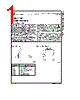
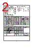
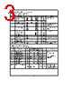

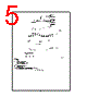
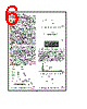
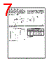
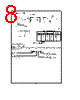

Okay, this is a hefty chunk of data! Let's break it down and summarize what we're looking at. This appears to be a datasheet excerpt for a CMOS integrated circuit, likely a buffer or driver. Here's a breakdown, organized by sections, with key takeaways and a final summary.
1. General Information (Implied):
️· Type: CMOS Integrated Circuit.
️· Application: Likely used as a buffer or driver – a circuit that takes a signal and amplifies or isolates it.
️· Operating Temperature Range: -55°C to 125°C. (b55°C to a125°C - the notation indicates temperature range)
️· Supply Voltage: The "VEE" parameter indicates a negative supply voltage of approximately -5.2V. VCC and VCCA are grounded (GND).
️· Reference Voltage: VREF is a reference voltage, around 1.55V to 1.15V.
2. DC Electrical Characteristics:
️· Power Supply Current (IEE): The circuit consumes a certain amount of power, depending on the temperature and the state of its pins (pins 6, 7 and 13 must be unconnected to obtain these numbers).
️· Input Voltages and Currents: Defines the allowable voltage ranges for the input pins (VIN), and the current that flows when the inputs are HIGH (IIH) or LOW (IIL).
️· Reference Voltage (VREF): Defined the voltage necessary to keep the reference operational.
3. AC Electrical Characteristics:
️· Propagation Delay (tPLH, tPHL): The time it takes for the output to respond to a change at the input. This is a critical performance parameter.
️· Setup and Hold Times (ts, th): Define the timing requirements for the input signals to be stable before and after the clock signal. These are critical for reliable operation.
️· Rise and Fall Times (tTLH, tTHL): How quickly the output signal transitions between HIGH and LOW states.
️· Maximum Clock Frequency (fMAX): The maximum frequency at which the circuit can reliably operate. (The numbers vary depending on temperature.)
Key Observations & Notes:
️· Negative Supply Voltage: The use of a negative supply voltage (-VEE) is somewhat unusual in modern circuits, but it might be necessary for specific biasing or performance requirements.
️· Temperature Dependence: Almost all the AC parameters (propagation delay, frequency) are temperature-dependent. The circuit's performance changes with temperature.
️· Timing Margins: The datasheet provides values for setup and hold times, which are important for ensuring that signals arrive at the circuit at the correct times.
️· Input Signal Characteristics: There are defined voltage levels that must be used for signals going into the component.
️· Specific Pin Requirements: Pins 6, 7 and 13 must be unconnected to obtain some electrical characteristics.
In Summary:
This data sheet excerpt describes the electrical characteristics of a CMOS buffer or driver operating with a negative supply voltage (-VEE) and a ground. The circuit is designed to operate over a wide temperature range (-55°C to 125°C), and its performance (particularly timing characteristics and frequency) varies with temperature. The datasheet provides essential information for designing circuits that use this component, including power consumption, input/output voltage levels, timing requirements, and frequency limits. The information is critical for engineers to ensure proper circuit operation and meet design specifications.
1. General Information (Implied):
️· Type: CMOS Integrated Circuit.
️· Application: Likely used as a buffer or driver – a circuit that takes a signal and amplifies or isolates it.
️· Operating Temperature Range: -55°C to 125°C. (b55°C to a125°C - the notation indicates temperature range)
️· Supply Voltage: The "VEE" parameter indicates a negative supply voltage of approximately -5.2V. VCC and VCCA are grounded (GND).
️· Reference Voltage: VREF is a reference voltage, around 1.55V to 1.15V.
2. DC Electrical Characteristics:
️· Power Supply Current (IEE): The circuit consumes a certain amount of power, depending on the temperature and the state of its pins (pins 6, 7 and 13 must be unconnected to obtain these numbers).
️· Input Voltages and Currents: Defines the allowable voltage ranges for the input pins (VIN), and the current that flows when the inputs are HIGH (IIH) or LOW (IIL).
️· Reference Voltage (VREF): Defined the voltage necessary to keep the reference operational.
3. AC Electrical Characteristics:
️· Propagation Delay (tPLH, tPHL): The time it takes for the output to respond to a change at the input. This is a critical performance parameter.
️· Setup and Hold Times (ts, th): Define the timing requirements for the input signals to be stable before and after the clock signal. These are critical for reliable operation.
️· Rise and Fall Times (tTLH, tTHL): How quickly the output signal transitions between HIGH and LOW states.
️· Maximum Clock Frequency (fMAX): The maximum frequency at which the circuit can reliably operate. (The numbers vary depending on temperature.)
Key Observations & Notes:
️· Negative Supply Voltage: The use of a negative supply voltage (-VEE) is somewhat unusual in modern circuits, but it might be necessary for specific biasing or performance requirements.
️· Temperature Dependence: Almost all the AC parameters (propagation delay, frequency) are temperature-dependent. The circuit's performance changes with temperature.
️· Timing Margins: The datasheet provides values for setup and hold times, which are important for ensuring that signals arrive at the circuit at the correct times.
️· Input Signal Characteristics: There are defined voltage levels that must be used for signals going into the component.
️· Specific Pin Requirements: Pins 6, 7 and 13 must be unconnected to obtain some electrical characteristics.
In Summary:
This data sheet excerpt describes the electrical characteristics of a CMOS buffer or driver operating with a negative supply voltage (-VEE) and a ground. The circuit is designed to operate over a wide temperature range (-55°C to 125°C), and its performance (particularly timing characteristics and frequency) varies with temperature. The datasheet provides essential information for designing circuits that use this component, including power consumption, input/output voltage levels, timing requirements, and frequency limits. The information is critical for engineers to ensure proper circuit operation and meet design specifications.
| Part No. | 11C90DC |
| Manufacturer | NSC |
| Size | 156 Kbytes |
| Pages | 10 pages |
| Description | 650 MHz Prescalers |
| ALLDATASHEET é útil para você? [ DONATE ] |
Sobre Alldatasheet | Publicidade | Contato conosco | Privacy Policy | Link para a ficha técnica | roca de Link | Lista de Fabricantes All Rights Reserved©Alldatasheet.com |
| Russian : Alldatasheetru.com | Korean : Alldatasheet.co.kr | Spanish : Alldatasheet.es | French : Alldatasheet.fr | Italian : Alldatasheetit.com Portuguese : Alldatasheetpt.com | Polish : Alldatasheet.pl | Vietnamese : Alldatasheet.vn Indian : Alldatasheet.in | Mexican : Alldatasheet.com.mx | British : Alldatasheet.co.uk | New Zealand : Alldatasheet.co.nz |
|
Family Site : ic2ic.com |
icmetro.com |
 Portuguese ▼
  English
 Chinese
 German
 Japanese
 Russian
 Korean
 Spanish
 French
 Italian
 Polish
 Vietnamese
 Indian
 Mexican
 British
 New Zealand