 |
Os motores de busca de Datasheet de Componentes eletrônicos |
|
|
Os motores de busca de Datasheet de Componentes eletrônicos |
|
The question interval is too short.
Please try again in a few seconds.

Hello, Please ask a question about MAX16909 Datasheet
# Example questions:
➢ What is the purpose of this network, and what components are typically used to create it?
➢ What is the primary function of the fsync pin, and what condition must be met for proper operation when an external signal is applied?
➢ What parameters are plotted on the y-axis of the 'vout vs. supply voltage (8v/400khz)' graphs, and what is the load condition for each graph?
| Part No. | MAX16909 |
| Manufacturer | MAXIM |
| Size | 2Mb |
| Pages | 18 pages |
| Description | 36V, 220kHz to 1MHz Step-Down Converter with Low Operating Current |




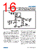
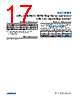


Okay, here's a summary of the information gleaned from the provided text, broken down into categories. I've aimed to extract the key technical details and design considerations.
1. Device Overview:
️· Part: MAX16909 - Step-Down Converter.
️· Function: Converts a higher voltage input to a lower output voltage.
️· Synchronization: Can synchronize its switching frequency to an external clock signal (FSYNC). The external clock *must* be 10% higher than the internal clock.
️· Switching Frequency Control: The switching frequency is adjustable using a resistor connected between FOSC and GND.
️· Standby Mode: Output voltage can be set between 3V and 5V during standby mode, powering internal circuitry.
2. Key Features & Pins:
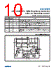
️· PGOOD: Open-drain output. Active-low. Indicates regulation status.
- Asserts (goes low) when VOUT is below 92.5% of its regulation point.
- Deasserts (goes high) when VOUT is above 95% of its regulation point.
️· OUT: Switch Regulator Output
️· FB (Feedback): Connected to a resistive divider from OUT to GND to set output voltage. Can be connected to BIAS to set output voltage to 5V.
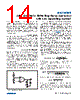
️· COMP (Compensation): Requires an RC network to GND for stable operation.
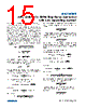
️· BIAS: Linear regulator output. Requires a 1µF bypass capacitor to ground.
️· BST (Bootstrap): Requires a 0.1µF capacitor between LX and BST.
️· FSYNC: Synchronization Input for external clock.
3. Design Considerations & Recommended Components:
️· Compensation Network: Essential for stable operation. Requires an RC network connected to COMP.
️· Bypass Capacitors: 1µF capacitor on BIAS, 0.1µF capacitor on BST.
️· Feedback Resistor Divider: Used to set the output voltage.
️· External Clock Frequency: If using FSYNC, it *must* be 10% higher than the internal clock frequency.
️· Regulation Points: PGOOD is linked to 92.5% and 95% regulation points.
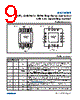
4. Pin Configurations (TSSOP, TQFN):
️· The text provides a table mapping pin numbers across different package types (TSSOP and TQFN) and their associated functions.
5. Test and Performance Data (Implied, but not fully explained):
️· The text includes several "Typical Operating Characteristics" graphs (V OUT vs. Temperature, V BIAS Load Regulation, I SHDN vs Temperature, V OUT vs Supply Voltage etc). These graphs depict device performance across various conditions (temperature, supply voltage, load). However, specific values are not fully explained.
Let me know if you'd like me to elaborate on any specific area, or if you have particular design questions based on this information.
1. Device Overview:
️· Part: MAX16909 - Step-Down Converter.
️· Function: Converts a higher voltage input to a lower output voltage.
️· Synchronization: Can synchronize its switching frequency to an external clock signal (FSYNC). The external clock *must* be 10% higher than the internal clock.
️· Switching Frequency Control: The switching frequency is adjustable using a resistor connected between FOSC and GND.
️· Standby Mode: Output voltage can be set between 3V and 5V during standby mode, powering internal circuitry.
2. Key Features & Pins:
️· PGOOD: Open-drain output. Active-low. Indicates regulation status.
- Asserts (goes low) when VOUT is below 92.5% of its regulation point.
- Deasserts (goes high) when VOUT is above 95% of its regulation point.
️· OUT: Switch Regulator Output
️· FB (Feedback): Connected to a resistive divider from OUT to GND to set output voltage. Can be connected to BIAS to set output voltage to 5V.
️· COMP (Compensation): Requires an RC network to GND for stable operation.
️· BIAS: Linear regulator output. Requires a 1µF bypass capacitor to ground.
️· BST (Bootstrap): Requires a 0.1µF capacitor between LX and BST.
️· FSYNC: Synchronization Input for external clock.
3. Design Considerations & Recommended Components:
️· Compensation Network: Essential for stable operation. Requires an RC network connected to COMP.
️· Bypass Capacitors: 1µF capacitor on BIAS, 0.1µF capacitor on BST.
️· Feedback Resistor Divider: Used to set the output voltage.
️· External Clock Frequency: If using FSYNC, it *must* be 10% higher than the internal clock frequency.
️· Regulation Points: PGOOD is linked to 92.5% and 95% regulation points.
4. Pin Configurations (TSSOP, TQFN):
️· The text provides a table mapping pin numbers across different package types (TSSOP and TQFN) and their associated functions.
5. Test and Performance Data (Implied, but not fully explained):
️· The text includes several "Typical Operating Characteristics" graphs (V OUT vs. Temperature, V BIAS Load Regulation, I SHDN vs Temperature, V OUT vs Supply Voltage etc). These graphs depict device performance across various conditions (temperature, supply voltage, load). However, specific values are not fully explained.
| Part No. | MAX16909 |
| Manufacturer | MAXIM |
| Size | 2Mb |
| Pages | 18 pages |
| Description | 36V, 220kHz to 1MHz Step-Down Converter with Low Operating Current |
| ALLDATASHEET é útil para você? [ DONATE ] |
Sobre Alldatasheet | Publicidade | Contato conosco | Privacy Policy | Link para a ficha técnica | roca de Link | Lista de Fabricantes All Rights Reserved©Alldatasheet.com |
| Russian : Alldatasheetru.com | Korean : Alldatasheet.co.kr | Spanish : Alldatasheet.es | French : Alldatasheet.fr | Italian : Alldatasheetit.com Portuguese : Alldatasheetpt.com | Polish : Alldatasheet.pl | Vietnamese : Alldatasheet.vn Indian : Alldatasheet.in | Mexican : Alldatasheet.com.mx | British : Alldatasheet.co.uk | New Zealand : Alldatasheet.co.nz |
|
Family Site : ic2ic.com |
icmetro.com |
 Portuguese ▼
  English
 Chinese
 German
 Japanese
 Russian
 Korean
 Spanish
 French
 Italian
 Polish
 Vietnamese
 Indian
 Mexican
 British
 New Zealand