|
Os motores de busca de Datasheet de Componentes eletrônicos |
|
|
Os motores de busca de Datasheet de Componentes eletrônicos |
|
OP07DDG4 Folha de dados(PDF) 7 Page - Texas Instruments |
|
|
|||||||||||||||||||||||||||||
OP07DDG4 Folha de dados(HTML) 7 Page - Texas Instruments |
|
|
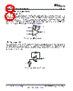
7 / 21 page  IN – IN+ VCC+ VCC – OUT OFFSET N1 OFFSET N2 Transistors 22 Resistors 11 Diode 1 Capacitor 1 Component Count OP07C, OP07D www.ti.com SLOS099G – OCTOBER 1983 – REVISED NOVEMBER 2014 9 Detailed Description 9.1 Overview These devices offer low offset and long-term stability by means of a low-noise, chopperless, bipolar-input- transistor amplifier circuit. For most applications, external components are not required for offset nulling and frequency compensation. The true differential input, with a wide input-voltage range and outstanding common- mode rejection, provides maximum flexibility and performance in high-noise environments and in noninverting applications. Low bias currents and extremely high input impedances are maintained over the entire temperature range. These devices are characterized for operation from 0°C to 70°C. 9.2 Functional Block Diagram 9.3 Feature Description 9.3.1 Offset-Voltage Null Capability The input offset voltage of operational amplifiers (op amps) arises from unavoidable mismatches in the differential input stage of the op-amp circuit caused by mismatched transistor pairs, collector currents, current- gain betas ( β), collector or emitter resistors, et cetera. The input offset pins allow the designer to adjust for these mismatches by external circuitry. See the Application and Implementation section for more details on design techniques. 9.3.2 Slew Rate The slew rate is the rate at which an operational amplifier can change its output when there is a change on the input. The OP07 has a 0.3-V/ μs slew rate. 9.4 Device Functional Modes The OP07 is powered on when the supply is connected. It can be operated as a single supply operational amplifier or dual supply amplifier depending on the application. Copyright © 1983–2014, Texas Instruments Incorporated Submit Documentation Feedback 7 Product Folder Links: OP07C OP07D |
|
|
Ligação URL |
| ALLDATASHEET é útil para você? [ DONATE ] |
Sobre Alldatasheet | Publicidade | Contato conosco | Privacy Policy | Link para a ficha técnica | roca de Link | Lista de Fabricantes All Rights Reserved©Alldatasheet.com |
| Russian : Alldatasheetru.com | Korean : Alldatasheet.co.kr | Spanish : Alldatasheet.es | French : Alldatasheet.fr | Italian : Alldatasheetit.com Portuguese : Alldatasheetpt.com | Polish : Alldatasheet.pl | Vietnamese : Alldatasheet.vn Indian : Alldatasheet.in | Mexican : Alldatasheet.com.mx | British : Alldatasheet.co.uk | New Zealand : Alldatasheet.co.nz |
|
Family Site : ic2ic.com |
icmetro.com |
 Portuguese ▼
 English
 Chinese
 German
 Japanese
 Russian
 Korean
 Spanish
 French
 Italian
 Portuguese
 Polish
 Vietnamese
 Indian
 Mexican
 British
 New Zealand