|
Os motores de busca de Datasheet de Componentes eletrônicos |
|
|
Os motores de busca de Datasheet de Componentes eletrônicos |
|
24C32-I/P Folha de dados(PDF) 6 Page - Microchip Technology |
|
|
|||||||||||||||||||||||||||||
24C32-I/P Folha de dados(HTML) 6 Page - Microchip Technology |
|
|
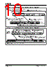
6 / 12 page  24C32 DS21061F-page 6 © 1996 Microchip Technology Inc. 4.0 WRITE OPERATION 4.1 Split Endurance The 24C32 is organized as a continuous 32K block of memory. However, the first 4K, starting at address 000, is rated at 10,000,000 E/W cycles guaranteed. The remainder of the array, 28K bits, is rated at 100K E/W cycles guaranteed. This feature is helpful in applica- tions in which some data change frequently, while a majority of the data change infrequently. One example would be a cellular telephone in which last-number redial and microcontroller scratch pad require a high- endurance block, while speed dials and lookup tables change infrequently and so require only a standard endurance rating. 4.2 Byte Write Following the start condition from the master, the con- trol code (four bits), the device select (three bits), and the R/W bit which is a logic low are clocked onto the bus by the master transmitter. This indicates to the addressed slave receiver that a byte with a word address will follow after it has generated an acknowl- edge bit during the ninth clock cycle. Therefore the next byte transmitted by the master is the high-order byte of the word address and will be written into the address pointer of the 24C32. The next byte is the least signifi- cant address byte. After receiving another acknowl- edge signal from the 24C32 the master device will transmit the data word to be written into the addressed memory location. The 24C32 acknowledges again and the master generates a stop condition. This initiates the internal write cycle, and during this time the 24C32 will not generate acknowledge signals (Figure 4-1). 4.3 Page Write The write control byte, word address and the first data byte are transmitted to the 24C32 in the same way as in a byte write. But instead of generating a stop condi- tion, the master transmits up to eight pages of eight data bytes each (64 bytes total) which are temporarily stored in the on-chip page cache of the 24C32. They will be written from cache into the EEPROM array after the master has transmitted a stop condition. After the receipt of each word, the six lower order address pointer bits are internally incremented by one. The higher order seven bits of the word address remain con- stant. If the master should transmit more than eight bytes prior to generating the stop condition (writing across a page boundary), the address counter (lower three bits) will roll over and the pointer will be incre- mented to point to the next line in the cache. This can continue to occur up to eight times or until the cache is full, at which time a stop condition should be generated by the master. If a stop condition is not received, the cache pointer will roll over to the first line (byte 0) of the cache, and any further data received will overwrite pre- viously captured data. The stop condition can be sent at any time during the transfer. As with the byte write operation, once a stop condition is received, an internal write cycle will begin. The 64-byte cache will continue to capture data until a stop condition occurs or the oper- ation is aborted (Figure 4-2). FIGURE 4-1: BYTE WRITE FIGURE 4-2: PAGE WRITE (FOR CACHE WRITE, SEE FIGURE 6-3) S t a r t Control Byte Word Address (1) Word Address (0) Data S t o p A C K A C K A C K A C K Bus Activity: Master SDA Line Bus Activity 0000 BUS MASTER SDA LINE BUS CONTROL BYTE WORD ADDRESS (1) S T O P S T A R T A C K 0 A C K A C K ACTIVITY ACTIVITY A C K A C K DATA n DATA n + 7 00 WORD ADDRESS (0) 0 |
|
|
Ligação URL |
| ALLDATASHEET é útil para você? [ DONATE ] |
Sobre Alldatasheet | Publicidade | Contato conosco | Privacy Policy | Link para a ficha técnica | roca de Link | Lista de Fabricantes All Rights Reserved©Alldatasheet.com |
| Russian : Alldatasheetru.com | Korean : Alldatasheet.co.kr | Spanish : Alldatasheet.es | French : Alldatasheet.fr | Italian : Alldatasheetit.com Portuguese : Alldatasheetpt.com | Polish : Alldatasheet.pl | Vietnamese : Alldatasheet.vn Indian : Alldatasheet.in | Mexican : Alldatasheet.com.mx | British : Alldatasheet.co.uk | New Zealand : Alldatasheet.co.nz |
|
Family Site : ic2ic.com |
icmetro.com |
 Portuguese ▼
 English
 Chinese
 German
 Japanese
 Russian
 Korean
 Spanish
 French
 Italian
 Portuguese
 Polish
 Vietnamese
 Indian
 Mexican
 British
 New Zealand