|
Os motores de busca de Datasheet de Componentes eletrônicos |
|
|
Os motores de busca de Datasheet de Componentes eletrônicos |
|
LT3653 Folha de dados(PDF) 7 Page - Linear Technology |
|
|
|||||||||||||||||||||||||||||
LT3653 Folha de dados(HTML) 7 Page - Linear Technology |
|
|
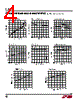
7 / 12 page  LT3653 7 3653f OPERATION Please refer to the Block Diagram. The LT3653 is specifi- cally tailored for use with a battery charger power path controller. The LT3653 regulates the high voltage input to a lower voltage to provide power to the system load and to the single-cell Li-Ion battery charger. High efficiency in the battery charger is achieved by keeping the voltage across it low. To accomplish this, the battery charger takes control of the LT3653 regulator control node, VC, and overrides the error amp, G1. The output voltage is regulated by the battery charger to a voltage slightly above the battery, typically 300mV. HVOK is a status pin which indicates to the charger that a high voltage input is present and that the LT3653 is ready to start providing power to the system load. When the HVOK pin is low, the LT3653 is not switching and the system output is not supported by the LT3653 regulator. The LT3653 is a constant frequency, current mode step down regulator. A switch cycle is initiated when the 1.5MHz oscillator enables the RS flip flop, turning on the internal power switch, Q1. The sense amplifier (A1) monitors the switch current via the voltage dropped across the current sense resistor RSENSE1. The compara- tor compares the amplified current signal with the output (VC) of the error amplifier (G1). The switch is turned off when this current exceeds a value determined by the VC voltage. The error amplifier monitors the VOUT volt- age through an internal resistor divider and, when not driven externally servos the VC voltage to regulate VOUT. If the VOUT voltage drops, the VC voltage will be driven higher increasing the output current and VOUT voltage. An active clamp (not shown) on the VC node provides current limit. The LT3653 is internally compensated with a pole zero combination. An external capacitor and internal diode, D2, are used to generate a voltage at the BOOST pin that is higher than the input supply. This allows the driver to fully saturate the internal bipolar NPN power switch for efficient operation. The switch driver operates from either VIN or BOOST to ensure startup. An internal regulator provides power to the control circuitry. This regulator includes input undervoltage and overvoltage protection which disables switching action when VIN is less than 7V and greater than 33V, typical. When switching is disabled, the LT3653 safely sustains input voltages up to 60V. Note that while switching is disabled the output will discharge. Output current limiting is provided via the servo action of amplifier G2. The voltage across the sense resistor, RSENSE2, is compared to a voltage programmed by ex- ternal resistor R1 on the ILIM pin. A capacitor averages the inductor ripple current. If the averaged inductor cur- rent exceeds the programmed value then the VC voltage is pulled low, reducing the current in the regulator. The output current limit circuit allows for lower current rated power path components and provides better control of system power dissipation. |
|
|
Ligação URL |
| ALLDATASHEET é útil para você? [ DONATE ] |
Sobre Alldatasheet | Publicidade | Contato conosco | Privacy Policy | Link para a ficha técnica | roca de Link | Lista de Fabricantes All Rights Reserved©Alldatasheet.com |
| Russian : Alldatasheetru.com | Korean : Alldatasheet.co.kr | Spanish : Alldatasheet.es | French : Alldatasheet.fr | Italian : Alldatasheetit.com Portuguese : Alldatasheetpt.com | Polish : Alldatasheet.pl | Vietnamese : Alldatasheet.vn Indian : Alldatasheet.in | Mexican : Alldatasheet.com.mx | British : Alldatasheet.co.uk | New Zealand : Alldatasheet.co.nz |
|
Family Site : ic2ic.com |
icmetro.com |
 Portuguese ▼
 English
 Chinese
 German
 Japanese
 Russian
 Korean
 Spanish
 French
 Italian
 Portuguese
 Polish
 Vietnamese
 Indian
 Mexican
 British
 New Zealand