|
Os motores de busca de Datasheet de Componentes eletrônicos |
|
|
Os motores de busca de Datasheet de Componentes eletrônicos |
|
AD668 Folha de dados(PDF) 15 Page - Analog Devices |
|
|
|||||||||||||||||||||||||||||
AD668 Folha de dados(HTML) 15 Page - Analog Devices |
|
|
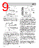
15 / 16 page  AD668 REV. A –15– bringing a latch clock pulse on board, whose opposite edge in- evitably produces a substantial glitch, even when the DAC is not supposed to be changing codes. Data Skew The AD668, like many of its slower predecessors, essentially uses each digital input line to switch a separate, weighted cur- rent to either the output (IOUT) or some other node (ANALOG COM). If the input bits are not changed simultaneously, or if the different DAC bits switch at different speeds, then the DAC output current will momentarily take on some incorrect value. This effect is particularly troublesome at the “carry points,” where the DAC output is to change by only one LSB, but sev- eral of the larger current sources must be switched to realize this change. Data skew can allow the DAC output to move a sub- stantial amount towards full scale or zero (depending upon the direction of the skew) when only a small transition is desired. Great care was taken in the design and layout of the AD668 to ensure that switching times of the DAC switches are symmetri- cal and that the length of the input data lines are short and well matched. The glitch-sensitive user should be equally diligent about minimizing the data skew at the AD668’s inputs, particu- larly for the 4 or 5 most significant bits. This can be achieved by using the proper logic family and gate to drive the DAC, and keeping the interconnect lines between the log outputs and the DAC inputs as short and as well matched as possible, particu- larly for the most significant bits. The top 6 bits should be driven from the same latch chip if latches are used. DEGLITCHING FOR PRECISION WAVEFORM GENERATION There are high speed SHAs available with specifications suffi- cient to deglitch the AD668, however most are hybrid in design at costs which can be prohibitive. A high performance, low cost alternative shown in Figure 27 is a discrete SHA utilizing a high speed monolithic op amp and high speed DMOS FET switches. This SHA circuit uses the inverting integrator architecture. The AD841 operational amplifier used (300 MHz gain bandwidth product) is fabricated on the same high speed process as the AD668. The time constant formed by the 100 Ω resistor and the 100 pF capacitor determines the acquisition time and also band limits the output signal to eliminate slew induced distortion. A discrete drive circuit is used to achieve the best performance from the SD5000 quad DMOS switch. This switch driving cell is composed of MPS571 RF npn transistors and an MC10124 TTL to ECL translator. Using this technique provides both high speed and highly symmetrical drive signals for the SD5000 switches. The switches are arranged in a single-throw double- pole (SPDT) configuration. The 360 pF “flyback” capacitor is switched to the op amp summing junction during the hold mode to keep switching transients from feeding to the output. This capacitor is grounded during sample mode to minimize its effect on acquisition time. Circuit layout for a high speed deglitcher is almost as critical as the design itself. Figure 28 shows the recommended layout of the deglitching cell for a double-sided printed circuit board. The layout is very compact with care taken that all critical signal paths are short. Performance of the AD668 in waveform generation applications is greatly improved with the use of this deglitching method. Peak harmonics and spurious free dynamic range are typically main- tained at -70 dB to -75 dB with update rates up to 10 MHz. 4 5 10 6 5 16 8 9 2 4 AD841 5V – 5V + MC 10124 15V – R11 20k TO PIN 2 SD5000 C1 0.039µF R12 1.6k S/H 5V – 5V – 15V – R6 249 R7 169 R8 510 R10 249 R9 169 R5 360 R4 360 MPS 571 (2) D1 IN4735 INPUT R1 100 R2 100 13 12 14 16 11 9 100pF C FILT 6 3 8 5 4 1 360pF CHOLD R3 100 OUTPUT 15V + Figure 27. High Performance, Low Cost Deglitching Circuit |
|
|
Ligação URL |
| ALLDATASHEET é útil para você? [ DONATE ] |
Sobre Alldatasheet | Publicidade | Contato conosco | Privacy Policy | Link para a ficha técnica | roca de Link | Lista de Fabricantes All Rights Reserved©Alldatasheet.com |
| Russian : Alldatasheetru.com | Korean : Alldatasheet.co.kr | Spanish : Alldatasheet.es | French : Alldatasheet.fr | Italian : Alldatasheetit.com Portuguese : Alldatasheetpt.com | Polish : Alldatasheet.pl | Vietnamese : Alldatasheet.vn Indian : Alldatasheet.in | Mexican : Alldatasheet.com.mx | British : Alldatasheet.co.uk | New Zealand : Alldatasheet.co.nz |
|
Family Site : ic2ic.com |
icmetro.com |
 Portuguese ▼
 English
 Chinese
 German
 Japanese
 Russian
 Korean
 Spanish
 French
 Italian
 Portuguese
 Polish
 Vietnamese
 Indian
 Mexican
 British
 New Zealand