|
Os motores de busca de Datasheet de Componentes eletrônicos |
|
|
Os motores de busca de Datasheet de Componentes eletrônicos |
|
MP7748DF Folha de dados(PDF) 15 Page - Monolithic Power Systems |
|
|
|||||||||||||||||||||||||||||
MP7748DF Folha de dados(HTML) 15 Page - Monolithic Power Systems |
|
|
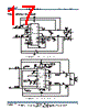
15 / 19 page  MP7748 – 2X20W STEREO SINGLE ENDED CLASS D AUDIO AMPLIFIER MP7748 Rev. 1.0 www.MonolithicPower.com 15 1/28/2011 MPS Proprietary Information. Patent Protected. Unauthorized Photocopy and Duplication Prohibited. © 2011 MPS. All Rights Reserved. to the MP7748 while blocking the DC voltage. Choose an input coupling capacitor such that the corner frequency (fIN) is less than the passband frequency. The corner frequency is calculated as: IN IN IN C R 2 1 f × × π × = Timer capacitor The start up source current slew rate is adjustable by selecting different capacitance of timer capacitor CTIMER. The larger the CTIMER capacitance is, the smaller the start up current slew rate is. It is recommended to use the CTIMER which capacitance is larger than 312nF, so the start up current slew rate would be smaller than 20mA/50ms which would help to eliminate the turn on pop. The recommended 2.2µF capacitor CTIMER results in a start up current slew rate of approximately 20mA/350ms. Power Source For maximum output power, the amplifier circuit requires a regulated external power source to supply the power to the amplifier. The higher the power supply voltage, the more power can be delivered to a given load resistance, however if the power source voltage exceeds the maximum voltage of 36V, the MP7748 may sustain damage. The power supply rejection of the MP7748 is excellent, however noise at the power supply can get to the output, so care must be taken to minimize power supply noise within the pass-band frequencies. Bypass the power supply with a large capacitor (typically aluminum electrolytic) along with a smaller 1µF ceramic capacitor at the MP7748 VDD supply pins. PCB Layout The circuit layout is critical for optimum performance and low output distortion and noise. It is highly recommended to duplicate EVB layout for optimum performance. If change is necessary, please follow these guidelines and take Figure 7 for references. 1) Place the following components as close to the MP7748 as possible: Bootstrap Cap CBS1 and CBS2 are used to supply the gate drive current to the internal high-side MOSFET. Place CBS1 as close to BST1/2 pin and SW1/2 pin as possible. Likewise, place CBS2 as close to BST2 pin and SW2 pins as possible. Power Supply Bypass Cap CBYP1 and CBYP2 carry the transient current for the switching power stage. To prevent overstressing of the MP7748 and excessive noise at the output, place CBYP1 as close to VDD1 pins and PGND1 pins as possible and also place CBYP2 as close to VDD2 pins and PGND2 pins as possible. Integral Capacitors CINT are used to set the amplifier switching frequencies and are typically on the order of a few nF. Place the integral capacitor CINT as close to the corresponding input as possible to reduce distortion and noise. For example, place CINT1 as close to pins 2 and 3 as possible at SE output configuration. Reference Bypass Capacitors For SE Output When used with SE output, CR1 and CR2 is needed to filter the ½ VDD reference voltages. Place CR1 and CR2 as close to the IC as possible to improve power supply rejection and reduce distortion and noise at the output. 2) The Inductor-Capacitor (LC) filter converts the pulse train at SW to the output voltage that drives the speaker. Please keep the filter capacitor close to the inductor. 3) When laying out the PCB, use two separate ground planes, analog ground (AGND) and power ground (PGND), and connect the two grounds together at a single point (usually around the bulk bypass capacitor) to prevent noise injection into the amplifier input to reduce distortion. 4) Keep the sensitive feedback signal trace on the input side and shield the trace with the AGND plane. Make sure that any traces carrying the switch node (SW) voltages are separated far from any input signal traces. If it is required to run the SW trace near the input, shield the input with a ground plane between the traces. Make sure that each channel is physically separated to prevent crosstalk. Make sure that all inductors used on a single circuit board have the same orientation. Also, make sure that the power supply is routed from the source to each channel individually, not serially. This prevents channel-to-channel |
|
|
Ligação URL |
| ALLDATASHEET é útil para você? [ DONATE ] |
Sobre Alldatasheet | Publicidade | Contato conosco | Privacy Policy | Link para a ficha técnica | roca de Link | Lista de Fabricantes All Rights Reserved©Alldatasheet.com |
| Russian : Alldatasheetru.com | Korean : Alldatasheet.co.kr | Spanish : Alldatasheet.es | French : Alldatasheet.fr | Italian : Alldatasheetit.com Portuguese : Alldatasheetpt.com | Polish : Alldatasheet.pl | Vietnamese : Alldatasheet.vn Indian : Alldatasheet.in | Mexican : Alldatasheet.com.mx | British : Alldatasheet.co.uk | New Zealand : Alldatasheet.co.nz |
|
Family Site : ic2ic.com |
icmetro.com |
 Portuguese ▼
 English
 Chinese
 German
 Japanese
 Russian
 Korean
 Spanish
 French
 Italian
 Portuguese
 Polish
 Vietnamese
 Indian
 Mexican
 British
 New Zealand