|
Os motores de busca de Datasheet de Componentes eletrônicos |
|
|
Os motores de busca de Datasheet de Componentes eletrônicos |
|
LTC3602 Folha de dados(PDF) 10 Page - Linear Technology |
|
|
|||||||||||||||||||||||||||||
LTC3602 Folha de dados(HTML) 10 Page - Linear Technology |
|
|
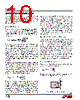
10 / 20 page  LTC3602 10 3602fb APPLICATIONS INFORMATION characteristics. The choice of which style inductor to use mainly depends on the price vs size requirements and any radiated field/EMI requirements. New designs for surface mount inductors are available from Coiltronics, Coilcraft, Toko and Sumida. CIN and COUT Selection The input capacitance, CIN, is needed to filter the trapezoi- dal current at the source of the top MOSFET. To prevent large ripple voltage, a low ESR input capacitor sized for the maximum RMS current should be used. RMS current is given by: II V V V V RMS OUT MAX OUT IN IN OUT = () •• – 1 This formula has a maximum at VIN = 2VOUT, where IRMS = IOUT/2. This simple worst-case condition is com- monly used for design because even significant deviations do not offer much relief. Note that ripple current ratings from capacitor manufacturers are often based on only 2000 hours of life which makes it advisable to further derate the capacitor, or choose a capacitor rated at a higher temperature than required. Several capacitors may also be paralleled to meet size or height requirements in the design. The selection of COUT is determined by the effective series resistance (ESR) that is required to minimize voltage ripple and load step transients, as well as the amount of bulk capacitance that is necessary to ensure that the control loop is stable. Loop stability can be checked by viewing the load transient response as described in a later section. The output ripple, ΔVOUT, is determined by: ΔV OUT ≤ΔIL •ESR + 1 8fC OUT ⎛ ⎝⎜ ⎞ ⎠⎟ The output ripple is highest at maximum input voltage since ΔIL increases with input voltage. Multiple capacitors placed in parallel may be needed to meet the ESR and RMS current handling requirements. Dry tantalum, special polymer, aluminum electrolytic and ceramic capacitors are all available in surface mount packages. Special polymer capacitors offer very low ESR but have lower capacitance density than other types. Tantalum capacitors have the highest capacitance density but it is important to only use types that have been surge tested for use in switching power supplies. Aluminum electrolytic capacitors have significantly higher ESR but can be used in cost-sensitive applications provided that consideration is given to ripple current ratings and long term reliability. Ceramic capacitors have excellent low ESR characteristics but can have a high voltage coefficient and audible piezoelectric effects. The high Q of ceramic capacitors with trace inductance can also lead to significant ringing. Using Ceramic Input and Output Capacitors Higher values, lower cost ceramic capacitors are now becoming available in smaller case sizes. Their high ripple current, high voltage rating and low ESR make them ideal for switching regulator applications. However, care must be taken when these capacitors are used at the input and output. When a ceramic capacitor is used at the input and the power is supplied by a wall adapter through long wires, a load step at the output can induce ringing at the input, VIN. At best, this ringing can couple to the output and be mistaken as loop instability. At worst, a sudden inrush of current through the long wires can potentially cause a voltage spike at VIN large enough to damage the part. Output Voltage Programming The output voltage is set by an external resistive divider according to the following equation: V OUT = 0.6V • 1+ R2 R1 ⎛ ⎝⎜ ⎞ ⎠⎟ The resistive divider allows the VFB pin to sense a fraction of the output voltage as shown in Figure 1. R2 LTC3602 R1 3602 F01 SGND VFB VOUT Figure 1. Setting the Output Voltage |
|
|
Ligação URL |
| ALLDATASHEET é útil para você? [ DONATE ] |
Sobre Alldatasheet | Publicidade | Contato conosco | Privacy Policy | Link para a ficha técnica | roca de Link | Lista de Fabricantes All Rights Reserved©Alldatasheet.com |
| Russian : Alldatasheetru.com | Korean : Alldatasheet.co.kr | Spanish : Alldatasheet.es | French : Alldatasheet.fr | Italian : Alldatasheetit.com Portuguese : Alldatasheetpt.com | Polish : Alldatasheet.pl | Vietnamese : Alldatasheet.vn Indian : Alldatasheet.in | Mexican : Alldatasheet.com.mx | British : Alldatasheet.co.uk | New Zealand : Alldatasheet.co.nz |
|
Family Site : ic2ic.com |
icmetro.com |
 Portuguese ▼
 English
 Chinese
 German
 Japanese
 Russian
 Korean
 Spanish
 French
 Italian
 Portuguese
 Polish
 Vietnamese
 Indian
 Mexican
 British
 New Zealand