|
Os motores de busca de Datasheet de Componentes eletrônicos |
|
|
Os motores de busca de Datasheet de Componentes eletrônicos |
|
AD9764ARUZ Folha de dados(PDF) 12 Page - Analog Devices |
|
|
|||||||||||||||||||||||||||||
AD9764ARUZ Folha de dados(HTML) 12 Page - Analog Devices |
|
|
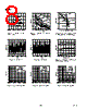
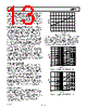
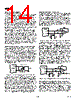
12 / 22 page  REV. B AD9764 –12– 1.25 V for an IOUTFS = 20 mA to 1.00 V for an IOUTFS = 2 mA. Operation beyond the positive compliance range will induce clipping of the output signal which severely degrades the AD9764’s linearity and distortion performance. For applications requiring the optimum dc linearity, IOUTA and/ or IOUTB should be maintained at a virtual ground via an I-V op amp configuration. Maintaining IOUTA and/or IOUTB at a virtual ground keeps the output impedance of the AD9764 fixed, signifi- cantly reducing its effect on linearity. However, it does not necessarily lead to the optimum distortion performance due to limitations of the I-V op amp. Note that the INL/DNL speci- fications for the AD9764 are measured in this manner using IOUTA. In addition, these dc linearity specifications remain virtually unaffected over the specified power supply range of 2.7 V to 5.5 V. Operating the AD9764 with reduced voltage output swings at IOUTA and IOUTB in a differential or single-ended output configu- ration reduces the signal dependency of its output impedance thus enhancing distortion performance. Although the voltage compliance range of IOUTA and IOUTB extends from –1.0 V to +1.25 V, optimum distortion performance is achieved when the maximum full-scale signal at IOUTA and IOUTB does not exceed approximately 0.5 V. A properly selected transformer with a grounded center-tap will allow the AD9764 to provide the re- quired power and voltage levels to different loads while main- taining reduced voltage swings at IOUTA and IOUTB. DC-coupled applications requiring a differential or single-ended output con- figuration should size RLOAD accordingly. Refer to Applying the AD9764 section for examples of various output configurations. The most significant improvement in the AD9764’s distortion and noise performance is realized using a differential output configuration. The common-mode error sources of both IOUTA and IOUTB can be substantially reduced by the common-mode rejection of a transformer or differential amplifier. These common-mode error sources include even-order distortion products and noise. The enhancement in distortion performance becomes more significant as the reconstructed waveform’s frequency content increases and/or its amplitude decreases. This is evident in Figure 14, which compares the differential vs. single-ended performance of the AD9764 at 50 MSPS for 0.0 and –6.0 dBFS single tone waveforms over frequency. The distortion and noise performance of the AD9764 is also slightly dependent on the analog and digital supply as well as the full-scale current setting, IOUTFS. Operating the analog supply at 5.0 V ensures maximum headroom for its internal PMOS current sources and differential switches leading to improved distortion performance as shown in Figure 8. Although IOUTFS can be set between 2 mA and 20 mA, selecting an IOUTFS of 20 mA will provide the best distortion and noise performance also shown in Figure 8. The noise performance of the AD9764 is affected by the digital supply (DVDD), output frequency, and increases with increasing clock rate as shown in Figure 13. Operating the AD9764 with low voltage logic levels between 3 V and 3.3 V will slightly reduce the amount of on-chip digital noise. In summary, the AD9764 achieves the optimum distortion and noise performance under the following conditions: (1) Differential Operation. (2) Positive voltage swing at IOUTA and IOUTB limited to +0.5 V. (3) IOUTFS set to 20 mA. (4) Analog Supply (AVDD) set at 5.0 V. (5) Digital Supply (DVDD) set at 3.0 V to 3.3 V with appro- priate logic levels. Note that the ac performance of the AD9764 is characterized under the above mentioned operating conditions. DIGITAL INPUTS The AD9764’s digital input consists of 14 data input pins and a clock input pin. The 14-bit parallel data inputs follow standard positive binary coding where DB13 is the most significant bit (MSB), and DB0 is the least significant bit (LSB). IOUTA pro- duces a full-scale output current when all data bits are at Logic 1. IOUTB produces a complementary output with the full-scale current split between the two outputs as a function of the input code. The digital interface is implemented using an edge-triggered master slave latch. The DAC output is updated following the rising edge of the clock as shown in Figure 1 and is designed to support a clock rate as high as 125 MSPS. The clock can be operated at any duty cycle that meets the specified latch pulse- width. The setup and hold times can also be varied within the clock cycle as long as the specified minimum times are met, although the location of these transition edges may affect digital feedthrough and distortion performance. Best performance is typically achieved when the input data transitions on the falling edge of a 50% duty cycle clock. The digital inputs are CMOS-compatible with logic thresholds, VTHRESHOLD, set to approximately half the digital positive supply (DVDD) or VTHRESHOLD = DVDD/2 ( ±20%) The internal digital circuitry of the AD9764 is capable of operating over a digital supply range of 2.7 V to 5.5 V. As a result, the digital inputs can also accommodate TTL levels when DVDD is set to accommodate the maximum high level voltage of the TTL drivers VOH(MAX). A DVDD of 3 V to 3.3 V will typically ensure proper compatibility with most TTL logic families. Figure 29 shows the equivalent digital input circuit for the data and clock inputs. The sleep mode input is similar with the exception that it contains an active pull-down circuit, thus ensuring that the AD9764 remains enabled if this input is left disconnected. DVDD DIGITAL INPUT Figure 29. Equivalent Digital Input |
|
|
Ligação URL |
| ALLDATASHEET é útil para você? [ DONATE ] |
Sobre Alldatasheet | Publicidade | Contato conosco | Privacy Policy | Link para a ficha técnica | roca de Link | Lista de Fabricantes All Rights Reserved©Alldatasheet.com |
| Russian : Alldatasheetru.com | Korean : Alldatasheet.co.kr | Spanish : Alldatasheet.es | French : Alldatasheet.fr | Italian : Alldatasheetit.com Portuguese : Alldatasheetpt.com | Polish : Alldatasheet.pl | Vietnamese : Alldatasheet.vn Indian : Alldatasheet.in | Mexican : Alldatasheet.com.mx | British : Alldatasheet.co.uk | New Zealand : Alldatasheet.co.nz |
|
Family Site : ic2ic.com |
icmetro.com |
 Portuguese ▼
 English
 Chinese
 German
 Japanese
 Russian
 Korean
 Spanish
 French
 Italian
 Portuguese
 Polish
 Vietnamese
 Indian
 Mexican
 British
 New Zealand