|
Os motores de busca de Datasheet de Componentes eletrônicos |
|
|
Os motores de busca de Datasheet de Componentes eletrônicos |
|
AD8065ART-REEL Folha de dados(PDF) 23 Page - Analog Devices |
|
|
|||||||||||||||||||||||||||||
AD8065ART-REEL Folha de dados(HTML) 23 Page - Analog Devices |
|
|
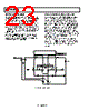
23 / 29 page  AD8065/AD8066 Rev. J | Page 22 of 28 THERMAL CONSIDERATIONS INPUT AND OUTPUT OVERLOAD BEHAVIOR With 24 V power supplies and 6.5 mA quiescent current, the AD8065 dissipates 156 mW with no load. The AD8066 dissipates 312 mW. This can lead to noticeable thermal effects, especially in the small SOT-23-5 (thermal resistance of 160°C/W). VOS temperature drift is trimmed to guarantee a maximum drift of 17 μV/°C, so it can change up to 0.425 mV due to warm-up effects for an AD8065/AD8066 in a SOT-23-5 package on 24 V. A simplified schematic of the AD8065/AD8066 input stage is shown in Figure 56. This shows the cascoded N-channel JFET input pair, the ESD and other protection diodes, and the auxiliary NPN input stage that eliminates any phase inversion behavior. When the common-mode input voltage to the amplifier is driven to within approximately 3 V of the positive power supply, the input JFET’s bias current turns off and the bias of the NPN pair turns on, taking over control of the amplifier. The NPN differential pair now sets the amplifier’s offset, and the input bias current is now in the range of several tens of microamps. This behavior is shown in Figure 32. Normal operation resumes when the common-mode voltage goes below the 3 V from the positive supply threshold. Ib increases by a factor of 1.7 for every 10°C rise in temperature. Ib is close to five times higher at 24 V supplies as opposed to a single 5 V supply. Heavy loads increase power dissipation and raise the chip junction temperature as described in the Maximum Power Dissipation section. Care should be taken not to exceed the rated power dissipation of the package. The output transistors of the rail-to-rail output stage have circuitry to limit the extent of their saturation when the output is overdriven. This helps output recovery time. Output recovery from a 0.5 V output overdrive on a ±5 V supply is shown in Figure 24. VTHRESHOLD VBIAS S VP TO REST OF AMP VCC S VN R1 Q2 Q5 Q3 Q1 Q6 Q7 Q4 R5 D1 R6 R3 R4 R2 R8 R7 D2 D3 D4 –VEE IT1 IT2 Figure 56. Simplified Input Stage |
|
Ligação URL |
| ALLDATASHEET é útil para você? [ DONATE ] |
Sobre Alldatasheet | Publicidade | Contato conosco | Privacy Policy | Link para a ficha técnica | roca de Link | Lista de Fabricantes All Rights Reserved©Alldatasheet.com |
| Russian : Alldatasheetru.com | Korean : Alldatasheet.co.kr | Spanish : Alldatasheet.es | French : Alldatasheet.fr | Italian : Alldatasheetit.com Portuguese : Alldatasheetpt.com | Polish : Alldatasheet.pl | Vietnamese : Alldatasheet.vn Indian : Alldatasheet.in | Mexican : Alldatasheet.com.mx | British : Alldatasheet.co.uk | New Zealand : Alldatasheet.co.nz |
|
Family Site : ic2ic.com |
icmetro.com |
 Portuguese ▼
 English
 Chinese
 German
 Japanese
 Russian
 Korean
 Spanish
 French
 Italian
 Portuguese
 Polish
 Vietnamese
 Indian
 Mexican
 British
 New Zealand