|
Os motores de busca de Datasheet de Componentes eletrônicos |
|
|
Os motores de busca de Datasheet de Componentes eletrônicos |
|
SSM2250RM Folha de dados(PDF) 8 Page - Analog Devices |
|
|
|||||||||||||||||||||||||||||
SSM2250RM Folha de dados(HTML) 8 Page - Analog Devices |
|
|
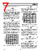
8 / 10 page  SSM2250 –8– REV. 0 Continuing from the previous example, the θ JA of the SSM2250 14-lead TSSOP package on a 4-layer board is 140 °C/W. To ensure the SSM2250 die junction temperature stays below 150 °C, the maximum ambient temperature can be solved using Equation 8. T 150 C P AMB, MAX JA DISS, MAX =+ ° − × θ =+ ° − ° × () 150 140 0 633 C C/W W . (8) =+ ° 61 C So the maximum ambient temperature must remain below 61 °C to protect the device against thermal damage. Another method for finding the maximum allowable ambient temperature is to use the power derating curve in Figure 15. The y-axis corresponds to the expected maximum power dissi- pation, and the x-axis is the corresponding maximum ambient temperature. Either method will return the same answer. AMBIENT TEMPERATURE – C 1.0 0.8 0 0 100 25 50 75 0.6 0.4 0.2 14-LEAD TSSOP JA = 140 C/W 10-LEAD MSOP JA = 180 C/W TJ,MAX = 150 C/W FREE AIR NO HEAT SINK Figure 15. Maximum Power Dissipation vs. Ambient Temperature Maximum Output Power The maximum amount of power that can be delivered to a speaker is a function of the supply voltage and the resistance of the speaker. Figure 15 shows the maximum BTL output power possible from the SSM2250. Maximum output power is defined as the point at which the output has greater than 1% distortion. SUPPLY VOLTAGE – V 1.5 5.0 2.0 2.5 3.0 3.5 4.0 4.5 1.6 0 1.4 0.8 0.6 0.4 0.2 1.2 1.0 RL = 4 RL = 8 RL = 16 Figure 16. Maximum BTL Output Power vs. VS To find the minimum supply voltage needed to achieve a speci- fied maximum undistorted output power, simply use Figure 16. The output power in SE mode is exactly one-fourth the equivalent output power in BTL mode. This is because twice the voltage swing across the two BTL outputs results in 4 the power delivered to the load. Figure 17 shows the maximum output power in SE mode vs. supply voltage for various headphone loads. SUPPLY VOLTAGE – V 1.5 5.0 2.0 2.5 3.0 3.5 4.0 4.5 100 0 50 25 75 RL = 32 RL = 64 RL = 128 Figure 17. Maximum SE Output Power vs. VS Example: An application requires only 500 mW to be output in BTL Mode into an 8 Ω speaker. By inspection, the minimum supply voltage required is 3.3 V. Speaker Efficiency and Loudness The effective loudness of 1 W of power delivered into an 8 Ω speaker is a function of the efficiency of the speaker. The efficiency of a speaker is typically rated at the sound pressure level (SPL) at 1 meter in front of the speaker with 1 W of power applied to the speaker. Most speakers are between 85 dB and 95 dB SPL at one meter at 1 W of power. Table I shows a comparison of the relative loudness of different sounds. Table I. Typical Sound Pressure Levels Source of Sound dB SPL Threshold of Pain 120 Heavy Street Traffic 95 Cabin of Jet Aircraft 80 Average Conversation 65 Average Home at Night 50 Quiet Recording Studio 30 Threshold of Hearing 0 It can be easily seen that 1 W of power into a speaker can produce quite a bit of acoustic energy. Shutdown Feature The SSM2250 can be put into a low power consumption shut- down mode by connecting Pin 3 to VDD. In shutdown mode, the SSM2250 has low supply current of 60 µA. Pin 3 should be connected to ground for normal operation. Con- necting Pin 3 to VDD will shut down all amplifiers and put all outputs into a high impedance state, effectively muting the SSM2250. A pull-up or pull-down resistor is not required. Pin 3 should never be left floating as this could produce unpredictable results. PC 99 Compliant Computer Audio Reference Design The schematic shown in Figure 18 is a reference design for a complete audio system in a computer. The design is compliant with the PC 99 standard for computer audio. |
|
|
Ligação URL |
| ALLDATASHEET é útil para você? [ DONATE ] |
Sobre Alldatasheet | Publicidade | Contato conosco | Privacy Policy | Link para a ficha técnica | roca de Link | Lista de Fabricantes All Rights Reserved©Alldatasheet.com |
| Russian : Alldatasheetru.com | Korean : Alldatasheet.co.kr | Spanish : Alldatasheet.es | French : Alldatasheet.fr | Italian : Alldatasheetit.com Portuguese : Alldatasheetpt.com | Polish : Alldatasheet.pl | Vietnamese : Alldatasheet.vn Indian : Alldatasheet.in | Mexican : Alldatasheet.com.mx | British : Alldatasheet.co.uk | New Zealand : Alldatasheet.co.nz |
|
Family Site : ic2ic.com |
icmetro.com |
 Portuguese ▼
 English
 Chinese
 German
 Japanese
 Russian
 Korean
 Spanish
 French
 Italian
 Portuguese
 Polish
 Vietnamese
 Indian
 Mexican
 British
 New Zealand