|
Os motores de busca de Datasheet de Componentes eletrônicos |
|
|
Os motores de busca de Datasheet de Componentes eletrônicos |
|
AD9709 Folha de dados(PDF) 9 Page - Analog Devices |
|
|
|||||||||||||||||||||||||||||
AD9709 Folha de dados(HTML) 9 Page - Analog Devices |
|
|
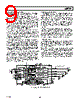
9 / 27 page  REV. 0 AD9709 –9– FUNCTIONAL DESCRIPTION Figure 20 shows a simplified block diagram of the AD9709. The AD9709 consists of two DACs, each one with its own independent digital control logic and full-scale output current control. Each DAC contains a PMOS current source array capable of providing up to 20 mA of full-scale current (IOUTFS). The array is divided into 31 equal currents that make up the five most significant bits (MSBs). The three lower bits consist of seven equal current sources whose value is 1/8th of an MSB current source. Implementing the lower bits with current sources, instead of an R-2R ladder, enhances the dynamic performance for multitone or low-amplitude signals and helps maintain the DACs high-output impedance (i.e., >100 k Ω). All of these current sources are switched to one or the other of the two output nodes (i.e., IOUTA or IOUTB) via PMOS differ- ential current switches. The switches are based on a new archi- tecture that drastically improves distortion performance. This new switch architecture reduces various timing errors and pro- vides matching complementary drive signals to the inputs of the differential current switches. The analog and digital sections of the AD9709 have separate power supply inputs (i.e., AVDD and DVDD) that can operate independently over a 3 V to 5.5 V range. The digital section, which is capable of operating up to a 125 MSPS clock rate, consists of edge-triggered latches and segment decoding logic circuitry. The analog section includes the PMOS current sources, the associated differential switches, a 1.20 V bandgap voltage reference and two reference control amplifiers. The full-scale output current of each DAC is regulated by sepa- rate reference control amplifiers and can be set from 2 mA to 20 mA via an external resistor, RSET, connected to the Full-Scale Adjust (FSADJ) pin. The external resistor, in combination with both the reference control amplifier and voltage reference VREFIO, sets the reference current IREF, which is replicated to the seg- mented current sources with the proper scaling factor. The full- scale current, IOUTFS, is 32 × IREF. REFERENCE OPERATION The AD9709 contains an internal 1.20 V bandgap reference. This can be easily overridden by an external reference with no effect on performance. REFIO serves as either an input or output depending on whether the internal or an external reference is used. To use the internal reference, simply decouple the REFIO pin to ACOM with a 0.1 µF capacitor. The internal reference voltage will be present at REFIO. If the voltage at REFIO is to be used elsewhere in the circuit, an external buffer amplifier with an input bias current of less than 100 nA should be used. An example of the use of the internal reference is shown in Figure 21. An external reference can be applied to REFIO as shown in Figure 22. The external reference may provide either a fixed reference voltage to enhance accuracy and drift performance or a varying reference voltage for gain control. Note that the 0.1 µF compensation capacitor is not required since the internal refer- ence is overridden, and the relatively high-input impedance of REFIO minimizes any loading of the external reference. GAINCTRL MODE The AD9709 allows the gain of each channel to be set indepen- dently by connecting one RSET resistor to FSADJ1 and another RSET resistor to FSADJ2. To add flexibility and reduce system cost, a single RSET resistor can be used to set the gain of both channels simultaneously. When GAINCTRL is low (i.e., connected to AGND), the inde- pendent channel gain control mode using two resistors is enabled. In this mode, individual RSET resistors should be connected to FSADJ1 and FSADJ2. When GAINCTRL is high (i.e., connected to AVDD), the master/slave channel gain control mode using one resistor is enabled. In this mode, a single RSET resistor is con- nected to FSADJ1 and the resistor on FSADJ2 can be removed. DIGITAL DATA INPUTS IREF1 IREF2 AVDD DB0-DB7 GAINCTRL WRT1/ IQWRT 1.2V REF RSET2 2k CHANNEL 1 LATCH CHANNEL 2 LATCH PMOS CURRENT SOURCE ARRAY PMOS CURRENT SOURCE ARRAY SEGMENTED SWITCHES FOR DAC1 SEGMENTED SWITCHES FOR DAC2 LSB SWITCH LSB SWITCH MULTIPLEXING LOGIC AD9709 DCOM MODE SLEEP CLK2/ IQRESET CLK1/ IQCLK 5V FSADJ1 RSET1 2k REFIO 0.1 F FSADJ2 DB0-DB7 WRT2/ IQSEL 5V DVDD DAC2 LATCH DAC1 LATCH CLK DIVIDER ACOM IOUTA1 IOUTB1 RL1A 50 VOUT1A RL1B 50 VOUT1B RL2A 50 VOUT2A RL2B 50 VOUT2B IOUTA2 IOUTB2 VDIFF = VOUTA – VOUTB Figure 20. Simplified Block Diagram |
|
Ligação URL |
| ALLDATASHEET é útil para você? [ DONATE ] |
Sobre Alldatasheet | Publicidade | Contato conosco | Privacy Policy | Link para a ficha técnica | roca de Link | Lista de Fabricantes All Rights Reserved©Alldatasheet.com |
| Russian : Alldatasheetru.com | Korean : Alldatasheet.co.kr | Spanish : Alldatasheet.es | French : Alldatasheet.fr | Italian : Alldatasheetit.com Portuguese : Alldatasheetpt.com | Polish : Alldatasheet.pl | Vietnamese : Alldatasheet.vn Indian : Alldatasheet.in | Mexican : Alldatasheet.com.mx | British : Alldatasheet.co.uk | New Zealand : Alldatasheet.co.nz |
|
Family Site : ic2ic.com |
icmetro.com |
 Portuguese ▼
 English
 Chinese
 German
 Japanese
 Russian
 Korean
 Spanish
 French
 Italian
 Portuguese
 Polish
 Vietnamese
 Indian
 Mexican
 British
 New Zealand