|
Os motores de busca de Datasheet de Componentes eletrônicos |
|
|
Os motores de busca de Datasheet de Componentes eletrônicos |
|
SL393D Folha de dados(PDF) 2 Page - System Logic Semiconductor |
|
|
|||||||||||||||||||||||||||||
SL393D Folha de dados(HTML) 2 Page - System Logic Semiconductor |
|
|
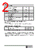
2 / 4 page  SL393 System Logic Semiconductor SLS MAXIMUM RATINGS * Symbol Parameter Value Unit VCC Power Supply Voltages Single Supply Split Supplies 36 ±18 V VIDR Input Differential Voltage Range 36 V VICR Input Common Mode Voltage Range (1) -0.3 to VCC V ISC Output Short Circuit to Ground Continuous IIN Input Current, per pin (2) 50 mA TJ Junction Temperature Plastic Packages 150 °C Tstg Storage Temperature -65 to +150 °C TL Lead Temperature, 1mm from Case for 10 Seconds 260 °C PD Power Dissipation @TA=25 °C Plastic Package Derate above 25 °C 570 5.7 µW mW/ °C *Maximum Ratings are those values beyond which damage to the device may occur. Functional operation should be restricted to the Recommended Operating Conditions. Notes: 1. Split Power Supplies. 2. VIN<-0.3V. This input current will only exist when voltage at any of the input leads is driven negative. RECOMMENDED OPERATING CONDITIONS Symbol Parameter Min Max Unit VCC DC Supply Voltage ±2.5 or 5.0 ±15 or 30 V TA Operating Temperature, All Package Types 0 +70 °C This device contains protection circuitry to guard against damage due to high static voltages or electric fields. However, precautions must be taken to avoid applications of any voltage higher than maximum rated voltages to this high-impedance circuit. For proper operation, VIN and VOUT should be constrained to the range GND ≤(V IN or VOUT) ≤V CC. Unused inputs must always be tied to an appropriate logic voltage level (e.g., either GND or VCC). Unused outputs must be left open. |
|
|
Ligação URL |
| ALLDATASHEET é útil para você? [ DONATE ] |
Sobre Alldatasheet | Publicidade | Contato conosco | Privacy Policy | Link para a ficha técnica | roca de Link | Lista de Fabricantes All Rights Reserved©Alldatasheet.com |
| Russian : Alldatasheetru.com | Korean : Alldatasheet.co.kr | Spanish : Alldatasheet.es | French : Alldatasheet.fr | Italian : Alldatasheetit.com Portuguese : Alldatasheetpt.com | Polish : Alldatasheet.pl | Vietnamese : Alldatasheet.vn Indian : Alldatasheet.in | Mexican : Alldatasheet.com.mx | British : Alldatasheet.co.uk | New Zealand : Alldatasheet.co.nz |
|
Family Site : ic2ic.com |
icmetro.com |
 Portuguese ▼
 English
 Chinese
 German
 Japanese
 Russian
 Korean
 Spanish
 French
 Italian
 Portuguese
 Polish
 Vietnamese
 Indian
 Mexican
 British
 New Zealand