ü
8-89
8
Preliminary
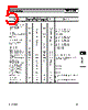
Product Description
Ordering Information
Typical Applications
Features
Functional Block Diagram
RF Micro Devices, Inc.
7628 Thorndike Road
Greensboro, NC 27409, USA
Tel (336) 664 1233
Fax (336) 664 0454
http://www.rfmd.com
Optimum Technology Matching® Applied
Si BJT
GaAs MESFET
GaAs HBT
Si Bi-CMOS
SiGe
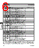
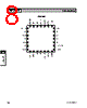
1
LNA VCC19
2
GND
5
LNA IN8
6
4
3
LNA IN19
7
GAIN SEL
14
13
12
11
10
9
8
15
VCC TX19
16
VCC DOUBLER
GND
17
IF A
18
20
GND
19
IF B
21
LO IN8
22
23
24
25
26
27
28
GND
GND
X2
RF2475
DUAL-BAND LOW NOISE AMPLIFIER/MIXER
WITH FREQUENCY DOUBLER
• TDMA Handsets
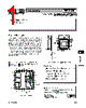
The RF2475 includes two downconverting mixers and
associated LNAs. It is designed for IS136 handset appli-
cations in the cellular 800MHz and PCS 1900MHz
bands. Each LNA has a gain bypass mode, which is con-
trolled by the gain select pin. The device internally ties the
two mixer outputs together, providing interface to a single
IF SAW filter. A frequency doubler is provided to supply
the LO signal to the PCS mixer and feeds the PCS trans-
mit LO output buffer. A cellular LO output buffer is also
included. The device is fabricated using Gallium Arsenide
HBT technology and is packaged in a 28-pin, 5mmx5mm
leadless package.
• Complete Dual-Band Receiver Front-End
• Stepped LNA Gain Control
• Integrated LO Frequency Doubler
• Integrated LO Output Buffers
• Meets IS136 Specifications
RF2475
Dual-Band Low Noise Amplifier/Mixer with Fre-
quency Doubler
RF2475 PCBA
Fully Assembled Evaluation Board
8
Rev A2 010918
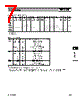
12°
MAX
1.00
0.85
0.65
0.30
4PLCS
0.50
0.23
0.13
4PLCS
5.00
sq.
2.50
Typ.
0.30
0.18
2
0.60
0.24
Typ
0.75
0.50
0.05
0.01
0.80
0.65
NOTES:
Shaded Pin is Lead 1.
1
Dimension applies to plated terminal: to be measured between 0.02 mm
and 0.25 mm from terminal end.
2
Pin 1 identifier must exist on top surface of package by identification
mark or feature on the package body. Exact shape and size is optional.
3
Package Warpage: 0.05 mm max.
4
Die Thickness Allowable: 0.305 mm max.
5
2.85
2.55
sq.
Package Style: LCC, 28-Pin, 5x5


 Portuguese ▼
 English
 Chinese
 German
 Japanese
 Russian
 Korean
 Spanish
 French
 Italian
 Portuguese
 Polish
 Vietnamese
 Indian
 Mexican
 British
 New Zealand