Features
1 of 4
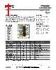
Optimum Technology
Matching® Applied
GaAs HBT
InGaP HBT
GaAs MESFET
SiGe BiCMOS
Si BiCMOS
SiGe HBT
GaAs pHEMT
Si CMOS
Si BJT
GaN HEMT
RF MICRO DEVICES®, RFMD®, Optimum Technology Matching®, Enabling Wireless Connectivity™, PowerStar®, POLARIS™ TOTAL RADIO™ and UltimateBlue™ are trademarks of RFMD, LLC. BLUETOOTH is a trade-
mark owned by Bluetooth SIG, Inc., U.S.A. and licensed for use by RFMD. All other trade names, trademarks and registered trademarks are the property of their respective owners. ©2006, RF Micro Devices, Inc.
Product Description
7628 Thorndike Road, Greensboro, NC 27409-9421 · For sales or technical
support, contact RFMD at (+1) 336-678-5570 or sales-support@rfmd.com.
InP HBT
LDMOS
RF MEMS
FPD2250
1.5W POWER pHEMT
The FPD2250 is an AlGaAs/InGaAs pseudomorphic High Electron Mobility Transis-
tor (pHEMT), featuring a 0.25
μmx2250μm Schottky barrier gate, defined by high-
resolution stepper-based photolithography. The recessed gate structure minimizes
parasitics to optimize performance. The epitaxial structure and processing have
been optimized for reliable high-power applications. The FPD2250 is also available
in the low-cost plastic SOT89 package.
32dBm Linear Output Power
at 12GHz
7.5dB Power Gain at 12GHz
42dBm OIP3
45% Power-Added Efficiency
Applications
Narrowband and Broadband
High-Performance Amplifiers
SATCOM Uplink Transmitters
PCS/Cellular Low-Voltage
High-Efficiency Output Ampli-
fiers
Medium-Haul Digital Radio
Transmitters
Rev A1 DS090612
Package Style: Bare Die
FPD22501.5W
Power pHEMT
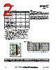
Parameter
Specification
Unit
Condition
Min.
Typ.
Max.
Electrical Specifications
P1dB Gain Compression
31.0
32.0
dBm
VDS=8V, IDS=50% IDSS
Maximum Stable Gain (S21/S12)
8.0
9.0
dB
VDS=8V, IDS=50% IDSS
Power Gain at P1dB (G1dB)6.5
7.5
dB
VDS=8V, IDS=50% IDSS
Power-Added Efficiency (PAE)
45
%
VDS=8V, IDS=50% IDSS, POUT=P1dB
OIP3
40
dBm
VDS=8V, IDS=50% IDSS
42
dBm
Matched for optimal power, tuned for best IP3
Saturated Drain-Source Current (IDSS)
560
700
825
mA
VDS=1.3V, VGS=0V
Maximum Drain-Source Current
(IMAX)
1125
mA
VDS=1.3V, VGS≈+1V
Transconductance (GM)
600
ms
VDS=1.3V, VGS=0V
Gate-Source Leakage Current (IGSO)10
μAVGS=-5V
Pinch-Off Voltage (VP)
|1.0|
V
VDS=1.3V, IDS=2.25mA
Gate-Source Breakdown Voltage
(VBDGS)
|12.0|
|14.0|
V
IGS=2.25mA
Gate-Drain Breakdown Voltage
(VBDGD)
|14.5|
|16.0|
V
IGD=2.25mA
Thermal Resistivity (
θJC)
30
°C/W
VDS>6V
Note: TAMBIENT=22°C, RF specifications measured at f=12GHz using CW signal.


 Portuguese ▼
 English
 Chinese
 German
 Japanese
 Russian
 Korean
 Spanish
 French
 Italian
 Portuguese
 Polish
 Vietnamese
 Indian
 Mexican
 British
 New Zealand