|
Os motores de busca de Datasheet de Componentes eletrônicos |
|
|
Os motores de busca de Datasheet de Componentes eletrônicos |
|
T15M64A Folha de dados(PDF) 9 Page - Taiwan Memory Technology |
|
|
|||||||||||||||||||||||||||||
T15M64A Folha de dados(HTML) 9 Page - Taiwan Memory Technology |
|
|
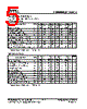
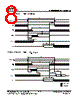
9 / 13 page  TE CH tm Preliminary T15M64A TM Technology Inc. reserves the right P. 9 Publication Date: SEP. 2002 to change products or specifications without notice. Revision:0.A Notes: 1. During this period, I/O pins are in the output state, so input signals of opposite phase to the outputs should not be applied. 2. The data output from D OUT are the same as the data written to D IN during the write cycle. 3. D OUT provides the read data for the next address. 4. Transition is measured ± 500 mV from steady state with C L = 5pF. This parameter is guaranteed but not 100% tested. 5. If OE is low during a WE controlled write cycle, the write pulse width must be the larger of tWP or (tWHZ + tDW) to allow the I/O drivers to turn off and data to be placed on the bus for the required tDW. If OE is high during a WE controlled write cycle, this requirement does not apply and the write pulse can be as short as the specified tWP. |
|
|
Ligação URL |
| ALLDATASHEET é útil para você? [ DONATE ] |
Sobre Alldatasheet | Publicidade | Contato conosco | Privacy Policy | Link para a ficha técnica | roca de Link | Lista de Fabricantes All Rights Reserved©Alldatasheet.com |
| Russian : Alldatasheetru.com | Korean : Alldatasheet.co.kr | Spanish : Alldatasheet.es | French : Alldatasheet.fr | Italian : Alldatasheetit.com Portuguese : Alldatasheetpt.com | Polish : Alldatasheet.pl | Vietnamese : Alldatasheet.vn Indian : Alldatasheet.in | Mexican : Alldatasheet.com.mx | British : Alldatasheet.co.uk | New Zealand : Alldatasheet.co.nz |
|
Family Site : ic2ic.com |
icmetro.com |
 Portuguese ▼
 English
 Chinese
 German
 Japanese
 Russian
 Korean
 Spanish
 French
 Italian
 Portuguese
 Polish
 Vietnamese
 Indian
 Mexican
 British
 New Zealand