|
Os motores de busca de Datasheet de Componentes eletrônicos |
|
|
Os motores de busca de Datasheet de Componentes eletrônicos |
|
KH300 Folha de dados(PDF) 5 Page - Cadeka Microcircuits LLC. |
|
|
|||||||||||||||||||||||||||||
KH300 Folha de dados(HTML) 5 Page - Cadeka Microcircuits LLC. |
|
|
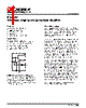
5 / 7 page  KH300 DATA SHEET REV. 1A January 2004 5 Layout Considerations To assure optimum performance the user should follow good layout practices which minimize the unwanted coupling of signals between nodes. During initial bread- boarding of the circuit, use direct point to point wiring, keeping lead lengths to less than 0.25”. The use of solid, unbroken ground plane is helpful. Avoid wire-wrap type pc boards and methods. Sockets with small, short pin receptacles may be used with minimal performance degradation although their use is not recommended. Figure 1: Recommended Non-inverting Gain Circuit Figure 2: Recommended Inverting Gain Circuit During pc board layout keep all traces short and direct. Rf and Rg should be as close as possible to pin 8 to minimize capacitance at that point. For the same reason, remove ground plane from the vicinity of pins 8 and 6. In other areas, use as much ground plane as possible on one side of the pc board. It is especially important to provide a ground return path for current from the load resistor to the power supply bypass capacitors. Ceramic capacitors of 0.01 to 0.1 µF should be close to pins 13 and 16. Larger tantalum capacitors should also be placed within one inch of these pins. To prevent signal distortion caused by reflections from impedance mis- matches, use terminated microstrip or coaxial cable when the signal must traverse more than a few inches. Since the pc board forms such an important part of the circuit, much time can be saved if prototype boards of any high frequency sections are built and tested early in the design phase. Controlling Bandwidth and Passband Response As with any op amp, the ratio of the two feedback resistors Rf and Rg, determines the gain of the KH300. Unlike conventional op amps, however, the closed loop pole- zero response of the KH300 is affected very little by the value of Rg. Rg scales the magnitude of the gain, but does not change the value of the feedback. Rf does influence the feedback and so the KH300 has been internally compensated for optimum performance with Rf = 1500Ω, but any value of Rf > 500Ω may be used with a single capacitor placed between pins 8 and 12 for compensation. See table 1. As Rf decreases, Cc must increase to maintain flat gain. Large values of Rf and Cc can be used together or separately to reduce the bandwidth. This may be desirable for reducing the noise bandwidth in applications not requiring the full fre- quency response available. Table 1: Bandwidth vs. Rf and Cc (Av = +20) Rf Cc f±0.3dB f-3.0dB (K Ω) (pF) (MHz) (MHz) 10.0 0 2 5 5.0 0 3 12 2.0 0 8 40 1.5 0 45 85 1.0 0.3 90 115 0.75 1.1 95 130 0.50 1.9 110 135 Low Gain Operation The small amount of stray capacitance present at the inverting input can cause peaking which increases with decreasing gain. The gain setting resistor Rg is effectively in parallel with this capacitance and so a frequency domain pole results. With small Rg (Gain > 8), this pole is at a high frequency and it affects the closed loop gain of the KH300 only slightly. At lower values of gain, this pole becomes significant. For example, at a gain of +2, the gain may peak as much as 3dB at 75MHz, and have a bandwidth exceeding 150MHz. The same behavior does not exist for low inverting gains, however, since the inverting input is a virtual ground which main- tains a constant voltage across the stray capacitance. Even at inverting gains << 1, the frequency response remains unchanged. 0.01 µF 22 µF -15 24 KH300 + - 8 Ri 50 Ω 6 Vin RL 50 Ω 1/2 Vo 16 13 11 +15 22 µF 0.01 µF 12 Rg Ro 50 Ω Av = 1 + Rf = 1500Ω (internal) Rf Rg 0.01 µF 22 µF -15 24 KH300 + - Ri 50 Ω Vin RL 50 Ω 1/2 Vo 16 13 11 +15 22 µF 0.01 µF 12 6 51 8 Rg Ro 50 Ω -Av = Rf = 1500Ω (internal) Rf Rg For Zin = 50Ω Select: Rg||Ri = 50 |
|
|
Ligação URL |
| ALLDATASHEET é útil para você? [ DONATE ] |
Sobre Alldatasheet | Publicidade | Contato conosco | Privacy Policy | Link para a ficha técnica | roca de Link | Lista de Fabricantes All Rights Reserved©Alldatasheet.com |
| Russian : Alldatasheetru.com | Korean : Alldatasheet.co.kr | Spanish : Alldatasheet.es | French : Alldatasheet.fr | Italian : Alldatasheetit.com Portuguese : Alldatasheetpt.com | Polish : Alldatasheet.pl | Vietnamese : Alldatasheet.vn Indian : Alldatasheet.in | Mexican : Alldatasheet.com.mx | British : Alldatasheet.co.uk | New Zealand : Alldatasheet.co.nz |
|
Family Site : ic2ic.com |
icmetro.com |
 Portuguese ▼
 English
 Chinese
 German
 Japanese
 Russian
 Korean
 Spanish
 French
 Italian
 Portuguese
 Polish
 Vietnamese
 Indian
 Mexican
 British
 New Zealand