|
Os motores de busca de Datasheet de Componentes eletrônicos |
|
|
Os motores de busca de Datasheet de Componentes eletrônicos |
|
LTC4403-1 Folha de dados(PDF) 7 Page - Linear Technology |
|
|
|||||||||||||||||||||||||||||
LTC4403-1 Folha de dados(HTML) 7 Page - Linear Technology |
|
|
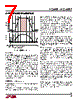
7 / 12 page  7 LTC4403-1/LTC4403-2 4403f APPLICATIO S I FOR ATIO Figure 1. LTC4403 Ramp Timing Demo Board The LTC4403-X demo board is available upon request. The demo board has a 900MHz and an 1800MHz RF channel and VHOLD controlled by the LTC4403-X. Timing signals for SHDN are generated on the board using a 13MHz crystal oscillator reference. The PCTL power control pin is driven by a 10-bit DAC and the DAC profile can be loaded via a serial port. The serial port data is stored in a flash memory which is capable of storing eight ramp profiles. The board is supplied preloaded with four GSM power profiles and four DCS power profiles covering the entire power range. External timing signals can be used in place of the internal crystal controlled timing. A power ramp software package is available which allows the user to create power control ramps. LTC4403 Control Loop Stability There are several factors that can improve or degrade loop frequency stability. 1) The additional voltage gain supplied by the RF power amplifier increases the loop gain, raising poles normally below the 0dB axis. The extra voltage gain can vary significantly over input/output power ranges, frequency, power supply, temperature and manufacturer. RF power amplifier gain control transfer functions are often not available and must be generated by the user. Loop oscil- lations are most likely to occur in the midpower range where the external voltage gain associated with the RF power amplifier typically peaks. It is useful to measure the oscillation or ringing frequency to determine whether it corresponds to the expected loop bandwidth and thus is due to high gain bandwidth. 2) Loop voltage losses supplied by the coupler network will improve phase margin. The larger the coupler loss the more stable the loop will become. However, larger losses reduce the RF signal to the LTC4403-X and detector performance may be degraded at low power levels. (See RF Detector Characteristics.) 3) Additional poles within the loop due to filtering or the turn-on response of the RF power amplifier can degrade the phase margin if these pole frequencies are near the effective loop bandwidth frequency. Generally loops using RF power amplifiers with fast turn-on times have more phase margin. Extra filtering below 16MHz should never be placed within the control loop, as this will only degrade phase margin. 4) Control loop instability can also be due to open loop issues. RF power amplifiers should first be characterized in an open loop configuration to ensure self oscillation is not present. Self-oscillation is often related to poor power supply decoupling, ground loops, coupling due to poor layout and extreme VSWR conditions. The oscillation fre- quency is generally in the 100kHz to 10MHz range. Power supply related oscillation suppression requires large value ceramic decoupling capacitors placed close to the RF power amp supply pins. The range of decoupling capacitor values is typically 1nF to 3.3 µF. 5) Poor layout techniques associated with the coupler network may result in high frequency signals bypassing the coupler. This could result in stability problems due to the reduction in the coupler loss. START CODE 200mV 10 –10 –20 –30 –40 –50 –60 –70 –80 11 µs MINIMUM, ALLOWS TIME FOR AUTOZERO TO SETTLE SHDN 0 543 553 561 571 4403 F01 –28 –18 –10 0 TIME ( µs) START PULSE ZERO CODE |
|
|
Ligação URL |
| ALLDATASHEET é útil para você? [ DONATE ] |
Sobre Alldatasheet | Publicidade | Contato conosco | Privacy Policy | Link para a ficha técnica | roca de Link | Lista de Fabricantes All Rights Reserved©Alldatasheet.com |
| Russian : Alldatasheetru.com | Korean : Alldatasheet.co.kr | Spanish : Alldatasheet.es | French : Alldatasheet.fr | Italian : Alldatasheetit.com Portuguese : Alldatasheetpt.com | Polish : Alldatasheet.pl | Vietnamese : Alldatasheet.vn Indian : Alldatasheet.in | Mexican : Alldatasheet.com.mx | British : Alldatasheet.co.uk | New Zealand : Alldatasheet.co.nz |
|
Family Site : ic2ic.com |
icmetro.com |
 Portuguese ▼
 English
 Chinese
 German
 Japanese
 Russian
 Korean
 Spanish
 French
 Italian
 Portuguese
 Polish
 Vietnamese
 Indian
 Mexican
 British
 New Zealand