|
Os motores de busca de Datasheet de Componentes eletrônicos |
|
|
Os motores de busca de Datasheet de Componentes eletrônicos |
|
ADA4859-3ACPZ-R2 Folha de dados(PDF) 14 Page - Analog Devices |
|
|
|||||||||||||||||||||||||||||
ADA4859-3ACPZ-R2 Folha de dados(HTML) 14 Page - Analog Devices |
|
|
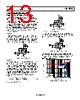
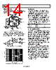
14 / 16 page  ADA4859-3 Rev. 0 | Page 14 of 16 VIDEO LINE DRIVER The ADA4859-3 was designed to excel in video driver applications. Figure 36 shows a typical schematic for a video driver operating on bipolar supplies. 1 2 3 4 11 12 CHARGE PUMP 10 9 56 7 8 16 15 14 13 1µF + 10µF 0.1µF +VS 1µF VIN (B) 75Ω 75Ω VOUT (B) 75Ω VOUT (G) 75Ω VOUT (R) 75Ω VIN (G) 75Ω VIN (R) PD Figure 36. Video Driver Schematic In applications that require multiple video loads be driven simultaneously, the ADA4859-3 can deliver. Figure 37 shows the ADA4856-3 configured with two video loads, and Figure 38 shows the large signal performance for multiple video loads. 75Ω CABLE 75Ω CABLE 75Ω 75Ω 75Ω 75Ω VOUT2 VOUT1 +VS 0.1µF 10µF VIN 75Ω CABLE 75Ω + – Figure 37. Video Driver Schematic for Two Video Loads 6.5 2.5 3.0 3.5 4.0 4.5 5.0 5.5 6.0 1 10 100 1000 FREQUENCY (MHz) RL = 150Ω RL = 75Ω Figure 38. Large Signal Frequency Response for Various Loads POWER-DOWN The ADA4859-3 is equipped with a PD (power-down) pin for all three amplifiers. This allows the user the ability to reduce the quiescent supply current when an amplifier is not active. The power-down threshold levels are derived from ground level. The amplifiers are powered down when the voltage applied to the PD pin is greater than a certain voltage from ground. In a 5 V supply application, the voltage is greater than 2 V, and in a 3.3 V supply application, the voltage is greater than 1.5 V. The amplifier is enabled whenever the PD pin is left floating (not connected). If the PD pin is not used, it is best to leave it floating or connected to ground. Note that the power-down feature does not control the charge pump output voltage and current. Table 5. Power-Down Voltage Control PD Pin 5 V 3.3 V Not Active <1.5 V <1 V Active >2 V >1.5 V LAYOUT CONSIDERATIONS As is the case with all high speed applications, careful attention to printed circuit board (PCB) layout details prevents associated board parasitics from becoming problematic. Proper RF design technique is mandatory. The PCB should have a ground plane covering all unused portions of the component side of the board to provide a low impedance return path. Removing the ground plane on all layers from the area near the input and output pins reduces stray capacitance. Locate termination resistors and loads as close as possible to their respective inputs and outputs. Keep input and output traces as far apart as possible to minimize coupling (crosstalk) through the board. Adherence to microstrip or stripline design techniques for long signal traces (greater than about 1 inch) is recommended. POWER SUPPLY BYPASSING Careful attention must be paid to bypassing the power supply pins of the ADA4859-3. Use high quality capacitors with low equivalent series resistance (ESR), such as multilayer ceramic capacitors (MLCCs), to minimize supply voltage ripple and power dissipation. A large, usually tantalum, 10 μF to 47 μF capacitor located in proximity to the ADA4859-3 is required to provide good decoupling for lower frequency signals. In addition, locate 0.1 μF MLCC decoupling capacitors as close to each of the power supply pins as is physically possible, no more than 1/8-inch away. The ground returns should terminate immediately into the ground plane. Locating the bypass capacitor return close to the load return minimizes ground loops and improves performance. |
|
|
Ligação URL |
| ALLDATASHEET é útil para você? [ DONATE ] |
Sobre Alldatasheet | Publicidade | Contato conosco | Privacy Policy | Link para a ficha técnica | roca de Link | Lista de Fabricantes All Rights Reserved©Alldatasheet.com |
| Russian : Alldatasheetru.com | Korean : Alldatasheet.co.kr | Spanish : Alldatasheet.es | French : Alldatasheet.fr | Italian : Alldatasheetit.com Portuguese : Alldatasheetpt.com | Polish : Alldatasheet.pl | Vietnamese : Alldatasheet.vn Indian : Alldatasheet.in | Mexican : Alldatasheet.com.mx | British : Alldatasheet.co.uk | New Zealand : Alldatasheet.co.nz |
|
Family Site : ic2ic.com |
icmetro.com |
 Portuguese ▼
 English
 Chinese
 German
 Japanese
 Russian
 Korean
 Spanish
 French
 Italian
 Portuguese
 Polish
 Vietnamese
 Indian
 Mexican
 British
 New Zealand