|
Os motores de busca de Datasheet de Componentes eletrônicos |
|
|
Os motores de busca de Datasheet de Componentes eletrônicos |
|
OPA544F/500 Folha de dados(PDF) 7 Page - Texas Instruments |
|
|
|||||||||||||||||||||||||||||
OPA544F/500 Folha de dados(HTML) 7 Page - Texas Instruments |
|
|
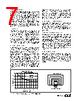
7 / 16 page  ® 7 OPA544 POWER DISSIPATION Power dissipation depends on power supply, signal and load conditions. For dc signals, power dissipation is equal to the product of output current times the voltage across the con- ducting output transistor. Power dissipation can be mini- mized by using the lowest possible power supply voltage necessary to assure the required output voltage swing. For resistive loads, the maximum power dissipation occurs at a dc output voltage of one-half the power supply voltage. Dissipation with ac signals is lower. Application Bulletin AB-039 explains how to calculate or measure power dissi- pation with unusual signals and loads. HEATSINKING Most applications require a heat sink to assure that the maximum junction temperature is not exceeded. The heat sink required depends on the power dissipated and on ambient conditions. Consult Application Bulletin AB-038 for information on determining heat sink requirements. The mounting tab of the surface-mount package version should be soldered to a circuit board copper area for good heat dissipation. Figure 3 shows typical thermal resistance from junction to ambient as a function of the copper area. THERMAL PROTECTION The OPA544 has thermal shutdown that protects the ampli- fier from damage. Any tendency to activate the thermal shutdown circuit during normal operation is indication of excessive power dissipation or an inadequate heat sink. The thermal protection activates at a junction temperature of approximately 155˚C. For reliable operation, junction tem- perature should be limited to 150˚C, maximum. To estimate the margin of safety in a complete design (including heat sink), increase the ambient temperature until the thermal protection is activated. Use worst-case load and signal con- ditions. For good reliability, the thermal protection should trigger more than 25˚C above the maximum expected ambi- ent condition of your application. This produces a junction temperature of 125˚C at the maximum expected ambient condition. Depending on load and signal conditions, the thermal pro- tection circuit may produce a duty-cycle modulated output signal. This limits the dissipation in the amplifier, but the rapidly varying output waveform may be damaging to some loads. The thermal protection may behave differently de- pending on whether internal dissipation is produced by sourcing or sinking output current. OUTPUT STAGE COMPENSATION The complex load impedances common in power op amp applications can cause output stage instability. Figure 3 shows an output series R/C compensation network (1 Ω in series with 0.01 µF) which generally provides excellent sta- bility. Some variation in circuit values may be required with certain loads. UNBALANCED POWER SUPPLIES Some applications do not require equal positive and negative output voltage swing. The power supply voltages of the OPA544 do not need to be equal. For example, a –6V negative power supply voltage assures that the inputs of the OPA544 are operated within their linear common-mode range, and that the output can swing to 0V. The V+ power supply could range from 15V to 65V. The total voltage (V– to V+) can range from 20V to 70V. With a 65V positive supply voltage, the device may not be protected from dam- age during short-circuits because of the larger VCE during this condition. OUTPUT PROTECTION Reactive and EMF-generating loads can return load current to the amplifier, causing the output voltage to exceed the power supply voltage. This damaging condition can be avoided with clamp diodes from the output terminal to the power supplies as shown in Figure 4. Fast-recovery rectifier diodes with a 4A or greater continuous rating are recom- mended. FIGURE 3. Thermal Resistance vs Circuit Board Copper Area. THERMAL RESISTANCE vs CIRCUIT BOARD COPPER AREA 50 40 30 20 10 0 012345 Copper Area (inches2) OPA544F Surface Mount Package 1oz copper Circuit Board Copper Area OPA544 Surface Mount Package |
|
|
Ligação URL |
| ALLDATASHEET é útil para você? [ DONATE ] |
Sobre Alldatasheet | Publicidade | Contato conosco | Privacy Policy | Link para a ficha técnica | roca de Link | Lista de Fabricantes All Rights Reserved©Alldatasheet.com |
| Russian : Alldatasheetru.com | Korean : Alldatasheet.co.kr | Spanish : Alldatasheet.es | French : Alldatasheet.fr | Italian : Alldatasheetit.com Portuguese : Alldatasheetpt.com | Polish : Alldatasheet.pl | Vietnamese : Alldatasheet.vn Indian : Alldatasheet.in | Mexican : Alldatasheet.com.mx | British : Alldatasheet.co.uk | New Zealand : Alldatasheet.co.nz |
|
Family Site : ic2ic.com |
icmetro.com |
 Portuguese ▼
 English
 Chinese
 German
 Japanese
 Russian
 Korean
 Spanish
 French
 Italian
 Portuguese
 Polish
 Vietnamese
 Indian
 Mexican
 British
 New Zealand