|
Os motores de busca de Datasheet de Componentes eletrônicos |
|
|
Os motores de busca de Datasheet de Componentes eletrônicos |
|
FIDO5210BBCZ-R7 Folha de dados(PDF) 18 Page - Analog Devices |
|
|
|||||||||||||||||||||||||||||
FIDO5210BBCZ-R7 Folha de dados(HTML) 18 Page - Analog Devices |
|
|
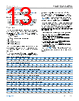
18 / 21 page  Data Sheet fido5100/fido5200 APPLICATIONS INFORMATION analog.com Rev. G | 18 of 21 Figure 11. Application for the REM Switch REM SWITCH HARDWARE The basic REM switch hardware is identified as the fido5100 or fido5200. For example, the fido5100 supports the following proto- cols: ► PROFINET RT and IRT, Class B and Class C ► EtherNet/IP with and without DLR, QuickConnect, CIP Sync, and CIP Motion ► Modbus TCP The fido5200 supports the following protocols: ► EtherCAT ► All protocols defined for the fido5100 The REM switches are PI Net Load Class III capable. It also supports IEEE 1588 Version 2 for ordinary clock (both peer to peer and end to end transparent clocks), raw frames, and user datagram protocol (UDP), as well as discovery configuration protocol (DCP), link layer discovery protocol (LLDP), dynamic host configuration protocol (DHCP), rapid spanning tree protocol (RSTP), virtual local area network (VLAN), and Internet group management protocol (IGMP) snooping support. REM Switch Drivers The REM switch driver for each protocol is provided as portable C code. The REM Switch Software Driver User Guide describes the driver for each protocol and its integration into a host processor. Refer to UG-1285 to download the user guide. BOARD LAYOUT The following guidelines provide best practice for board layout with the REM switch: ► Use individual polygons for the power planes for each of the three supplies. Allow at least 0.2 mm of isolation between the power planes. ► Isolate clock signals from the other traces and make them as short as possible. ► A minimum clearance around the REM switch of 3 mm is re- quired to facilitate heat dissipation. DESIGN CONSIDERATIONS Power The REM switch require 1.2 V and 3.3 V power supplies. Each power level requires its own power plane on the PCB. The REM switch uses 3.3 V LVCMOS logic levels for its I/O. This I/O requires a 3.3 V (±10%) power supply circuit. Ideally, this circuit uses a low noise switching power supply. The REM switch use a 1.2 V (±10%) supply for the core of the chip. The core power supply requires its own power plane on the PCB. Additional best practices include ► Use one 0.1 µF bypass capacitor for every 1.2 V power pin. ► Use a power supply IC rated to supply at least 100 mA. ► Supply 3.3 V power from its own layer on the PCB to the 3.3 V power input pins on the REM switch. ► Use one 0.1 µF bypass capacitor for every 3.3 V power pin. ► For the 1.2 V analog supply, the signal must be isolated using a 120 Ω, 500 mA ferrite bead and 10 µF, 1 µF, and 0.1 µF filtering capacitors. Reset The RESET signal is typically driven by the host microprocessor that is paired with the REM switch. RESET is an active low signal; therefore, pull RESET high as power becomes valid. Physical Layer (PHY) The REM switch is designed intentionally without PHYs because of the different requirements on PHY performance. EtherCAT and PROFINET IRT have much tighter latency and jitter requirements than standard Ethernet. The ADIN1200 is a low power, single port, 10 Mbps, and 100 Mbps Ethernet PHY. It is designed for industrial Ethernet applications and pairs well with fido® devices where a PHY is needed. Clocking Most PHYs allow the user to clock the PHY with a crystal oscillator or a separate clock source when using an MII interface. It is a |
|
|
Ligação URL |
| ALLDATASHEET é útil para você? [ DONATE ] |
Sobre Alldatasheet | Publicidade | Contato conosco | Privacy Policy | Link para a ficha técnica | roca de Link | Lista de Fabricantes All Rights Reserved©Alldatasheet.com |
| Russian : Alldatasheetru.com | Korean : Alldatasheet.co.kr | Spanish : Alldatasheet.es | French : Alldatasheet.fr | Italian : Alldatasheetit.com Portuguese : Alldatasheetpt.com | Polish : Alldatasheet.pl | Vietnamese : Alldatasheet.vn Indian : Alldatasheet.in | Mexican : Alldatasheet.com.mx | British : Alldatasheet.co.uk | New Zealand : Alldatasheet.co.nz |
|
Family Site : ic2ic.com |
icmetro.com |
 Portuguese ▼
 English
 Chinese
 German
 Japanese
 Russian
 Korean
 Spanish
 French
 Italian
 Portuguese
 Polish
 Vietnamese
 Indian
 Mexican
 British
 New Zealand