Os motores de busca de Datasheet de Componentes eletrônicos
  Portuguese  ▼
ALLDATASHEETPT.COM

X  

RF2638PCBA-PCS/CEL Folha de dados(PDF) 3 Page - RF Micro Devices

Nome de Peças RF2638PCBA-PCS/CEL
Descrição Electrónicos  W-CDMA AND CDMA UPCONVERTER/ BPSK MODULATOR
PDF  10 Pages
Scroll/Zoom Zoom In 100%  Zoom Out
Fabricante Electrônico  RFMD [RF Micro Devices]
Página de início  http://www.rfmd.com
Logo RFMD - RF Micro Devices

RF2638PCBA-PCS/CEL Folha de dados(HTML) 3 Page - RF Micro Devices

  RF2638PCBA-PCS/CEL Datasheet HTML 1Page - RF Micro Devices RF2638PCBA-PCS/CEL Datasheet HTML 2Page - RF Micro Devices RF2638PCBA-PCS/CEL Datasheet HTML 3Page - RF Micro Devices RF2638PCBA-PCS/CEL Datasheet HTML 4Page - RF Micro Devices RF2638PCBA-PCS/CEL Datasheet HTML 5Page - RF Micro Devices RF2638PCBA-PCS/CEL Datasheet HTML 6Page - RF Micro Devices RF2638PCBA-PCS/CEL Datasheet HTML 7Page - RF Micro Devices RF2638PCBA-PCS/CEL Datasheet HTML 8Page - RF Micro Devices RF2638PCBA-PCS/CEL Datasheet HTML 9Page - RF Micro Devices Next Button
Zoom Inzoom in Zoom Outzoom out
 3 / 10 page
background image
6-29
RF2638
Rev B15 060921
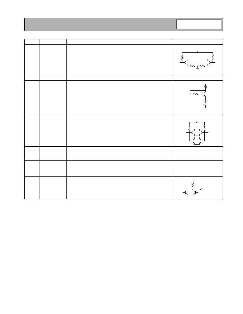
Pin
Function
Description
Interface Schematic
1IF-
Balanced IF input pin. This pin is internally DC-biased and should be
DC-blocked if connected to a device with a DC level present. For single-
ended input operation, one pin is used as an input and the other IF
input is AC-coupled to ground. The balanced, input impedance is
260
Ω.
2IF+
Same as pin 1, except complementary input.
See pin 1.
3BYP
Bypass pin for internal bias circuitry. Bypass with a 1nF capacitor.
4LO-
Balanced LO input pin. This pin is internally DC-biased and should be
DC-blocked if connected to a device with a DC level present. For single-
ended input operation, one pin is used as an input and the other LO
input is AC-coupled to ground.
5LO+
Same as pin 4, except complementary input.
See pin 4.
6GND
Ground connection. For best performance, keep traces physically short
and connect immediately to ground plane.
7VCC
Supply voltage pin. External bypassing is required. External RF, LO,
and IF bypassing is required. The trace length between the pin and the
bypass capacitors should be minimized. The ground side of the bypass
capacitors should connect immediately to ground plane.
8RF OUT
RF output pin.
IF+
IF-
130
Ω
130
Ω
BIAS
BYP
LO+
LO-
BIAS
300
Ω
RF OUT


Html Pages

1 2 3 4 5 6 7 8 9 10


Folha de dados Download

Go To PDF Page


Ligação URL


ALLDATASHEET é útil para você?  [ DONATE ] 

Sobre Alldatasheet   |   Publicidade   |   Contato conosco   |   Privacy Policy   |   Link para a ficha técnica    |   roca de Link   |   Lista de Fabricantes
All Rights Reserved©Alldatasheet.com


Mirror Sites
English : Alldatasheet.com  |   English : Alldatasheet.net  |   Chinese : Alldatasheetcn.com  |   German : Alldatasheetde.com  |   Japanese : Alldatasheet.jp
Russian : Alldatasheetru.com  |   Korean : Alldatasheet.co.kr  |   Spanish : Alldatasheet.es  |   French : Alldatasheet.fr  |   Italian : Alldatasheetit.com
Portuguese : Alldatasheetpt.com  |   Polish : Alldatasheet.pl  |   Vietnamese : Alldatasheet.vn
Indian : Alldatasheet.in  |   Mexican : Alldatasheet.com.mx  |   British : Alldatasheet.co.uk  |   New Zealand : Alldatasheet.co.nz
Family Site : ic2ic.com  |   icmetro.com