9 / 30 page
9 of 30
RF2489
Rev A21 DS070308
7628 Thorndike Road, Greensboro, NC 27409-9421 · For sales or technical
support, contact RFMD at (+1) 336-678-5570 or sales-support@rfmd.com.
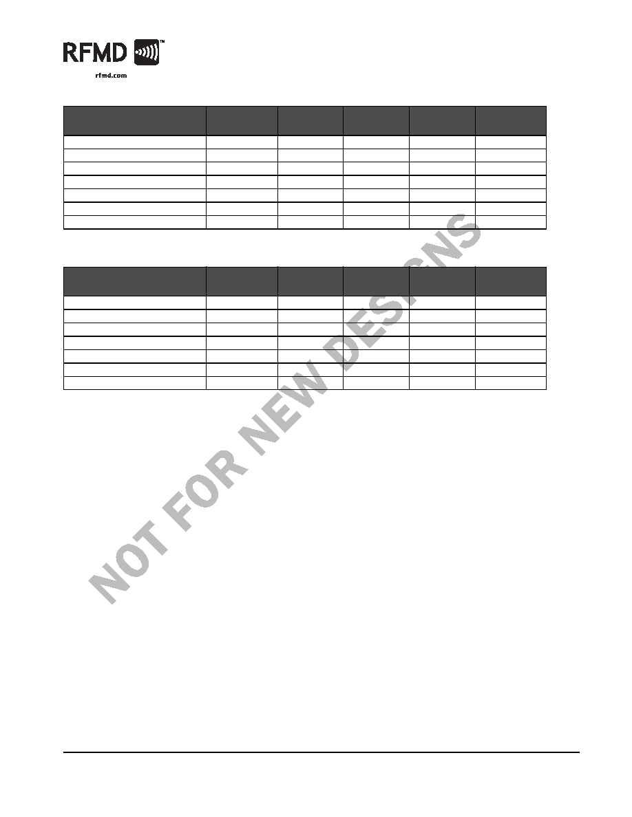
Control Logic (Single VCO)
Control Logic (Dual VCO)
Application Note 1
The PCS TX LO output pin (pin 7) and the CELL TX LO output pin (pin 8) can be combined. When BAND SEL is set low, the PCS
band LO limiter and PCS TX LO buffer are off. Also, when BAND SEL is set high, the cellular band LO limiter and frequency
divider are off as well as the cellular TX LO buffer. The LO leakage through the path of the disabled LO limiter/divider and TX LO
buffer is insignificant.
Typical LO isolation test data follows:
LO Input Frequency=2128MHz, PIN=-4dBm, BAND SEL=0, /2 SELECT=1
POUTPIN8=-28dBm at 2128MHz
POUTPIN8=-11dBm at 1064MHz
POUTPIN7=-34dBm at 2128MHz
Mode
BAND SEL
IF SEL
ENABLE
TX BUFF
ENABLE
/2 SELECT
Cellular FM
0
1
1
X
1
Cellular CDMA
0
0
1
X
1
PCS CDMA
1
0
1
X
X
Power Down
1
1
1
X
X
Power Down 2
X
X
0
X
X
TX Buffer Enabled
X
X
1
1
X
/2 Enabled
0
X
1
X
1
Mode
BAND SEL
IF SEL
ENABLE
TX BUFF
ENABLE
/2 SELECT
Cellular FM
0
1
1
X
0
Cellular CDMA
0
0
1
X
0
PCS CDMA
1
0
1
X
X
Power Down
1
1
1
X
X
Power Down 2
X
X
0
X
X
TX Buffer Enabled
X
X
1
1
X
/2 Enabled
0
X
1
X
1

 Portuguese ▼
 English
 Chinese
 German
 Japanese
 Russian
 Korean
 Spanish
 French
 Italian
 Portuguese
 Polish
 Vietnamese
 Indian
 Mexican
 British
 New Zealand