|
Os motores de busca de Datasheet de Componentes eletrônicos |
|
|
Os motores de busca de Datasheet de Componentes eletrônicos |
|
MCP6241 Folha de dados(PDF) 10 Page - Microchip Technology |
|
|
|||||||||||||||||||||||||||||
MCP6241 Folha de dados(HTML) 10 Page - Microchip Technology |
|
|
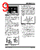
10 / 28 page  MCP6241/2/4 DS21882C-page 10 © 2005 Microchip Technology Inc. 4.7 Application Circuits 4.7.1 MATCHING THE IMPEDANCE AT THE INPUTS To minimize the effect of offset voltage in an amplifier circuit, the impedances at the inverting and non- inverting inputs need to be matched. This is done by choosing the circuit resistor values so that the total resistance at each input is the same. Figure 4-7 shows a summing amplifier circuit. FIGURE 4-7: Summing Amplifier Circuit. To match the inputs, set all voltage sources to ground and calculate the total resistance at the input nodes. In this summing amplifier circuit, the resistance at the inverting input is calculated by setting VIN1, VIN2 and VOUT to ground. In this case, RG1, RG2 and RF are in parallel. The total resistance at the inverting input is: At the non-inverting input, VDD is the only voltage source. When VDD is set to ground, both RX and RY are in parallel. The total resistance at the non-inverting input is: To minimize offset voltage and increase circuit accuracy, the resistor values need to meet the condition: 4.7.2 COMPENSATING FOR THE PARASITIC CAPACITANCE In analog circuit design, the PCB parasitic capacitance can compromise the circuit behavior; Figure 4-8 shows a typical scenario. If the input of an amplifier sees parasitic capacitance of several picofarad (CPARA, which includes the common mode capacitance of 6 pF, typical) and large RF and RG,the frequency response of the circuit will include a zero. This parasitic zero introduces gain peaking and can cause circuit instability. FIGURE 4-8: Effect of Parasitic Capacitance at the Input. One solution is to use smaller resistor values to push the zero to a higher frequency. Another solution is to compensate by introducing a pole at the point at which the zero occurs. This can be done by adding CF in parallel with the feedback resistor (RF). CF needs to be selected so that the ratio CPARA:CF is equal to the ratio of RF:RG. MCP624X VOUT VIN2 – + VIN1 RG2 RG1 RF RZ VDD RX RY R VIN – 1 1 R G1 --------- 1 R G2 --------- 1 R F ------ ++ ⎝⎠ ⎛⎞ --------------------------------------------- = Where: RVIN– = total resistance at the inverting input R VIN+ 1 1 R X ------ 1 R Y ------ + ⎝⎠ ⎛⎞ ------------------------- R Z + = Where: RVIN+ = total resistance at the inverting input R VIN+ R VIN – = VOUT CF VDC + – VAC RG RF CPARA C F C PARA R G R F ------- • = MCP624X |
|
Ligação URL |
| ALLDATASHEET é útil para você? [ DONATE ] |
Sobre Alldatasheet | Publicidade | Contato conosco | Privacy Policy | Link para a ficha técnica | roca de Link | Lista de Fabricantes All Rights Reserved©Alldatasheet.com |
| Russian : Alldatasheetru.com | Korean : Alldatasheet.co.kr | Spanish : Alldatasheet.es | French : Alldatasheet.fr | Italian : Alldatasheetit.com Portuguese : Alldatasheetpt.com | Polish : Alldatasheet.pl | Vietnamese : Alldatasheet.vn Indian : Alldatasheet.in | Mexican : Alldatasheet.com.mx | British : Alldatasheet.co.uk | New Zealand : Alldatasheet.co.nz |
|
Family Site : ic2ic.com |
icmetro.com |
 Portuguese ▼
 English
 Chinese
 German
 Japanese
 Russian
 Korean
 Spanish
 French
 Italian
 Portuguese
 Polish
 Vietnamese
 Indian
 Mexican
 British
 New Zealand