|
Os motores de busca de Datasheet de Componentes eletrônicos |
|
|
Os motores de busca de Datasheet de Componentes eletrônicos |
|
UCD3138064RGCT Folha de dados(PDF) 4 Page - Texas Instruments |
|
|
|
|||||||||||||||||||||||||||||
UCD3138064RGCT Folha de dados(HTML) 4 Page - Texas Instruments |
|
|
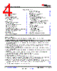
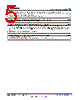
4 / 104 page  Table of Contents 1 Features............................................................................1 2 Applications..................................................................... 1 3 Description.......................................................................2 4 Functional Block Diagram.............................................. 3 5 Revision History.............................................................. 4 6 Device Options................................................................ 6 6.1 Device Comparison Table........................................... 6 6.2 Product Selection Matrix............................................. 6 7 Pin Configuration and Functions...................................8 7.1 Pin Diagrams.............................................................. 8 7.2 Pin Functions.............................................................. 9 8 Specifications................................................................ 12 8.1 Absolute Maximum Ratings (1) .................................12 8.2 Handling Ratings.......................................................12 8.3 Recommended Operating Conditions.......................12 8.4 Thermal Information..................................................13 8.5 Electrical Characteristics...........................................14 8.6 Timing Characteristics...............................................16 8.7 PMBus/SMBus/I2C Timing........................................ 18 8.8 Power On Reset (POR) / Brown Out Reset (BOR)...19 8.9 Typical Clock Gating Power Savings........................ 20 8.10 Typical Characteristics............................................ 21 9 Detailed Description......................................................22 9.1 Overview................................................................... 22 9.2 Functional Block Diagram......................................... 23 9.3 Feature Description...................................................24 9.4 Device Functional Modes..........................................49 9.5 Memory..................................................................... 57 10 Applications and Implementation.............................. 61 10.1 Application Information........................................... 61 10.2 Typical Application.................................................. 62 11 Power Supply Recommendations..............................73 11.1 Introduction To Power Supply and Layout Recommendations...................................................... 73 11.2 3.3-V Supply Pins....................................................73 11.3 Recommendation for V33 Ramp up Slew Rate for UCD3138 and UCD3138064..................................73 11.4 Recommendation for RC Time Constant of RESET Pin for UCD3138 and UCD3138064.............. 74 12 Layout...........................................................................77 12.1 Layout Guidelines................................................... 77 12.2 Layout Example...................................................... 82 13 Device and Documentation Support..........................87 13.1 Device Support....................................................... 87 13.2 Documentation Support.......................................... 88 13.3 Trademarks.............................................................88 13.4 Electrostatic Discharge Caution..............................88 13.5 Glossary..................................................................88 14 Mechanical, Packaging, and Orderable Information.................................................................... 88 5 Revision History NOTE: Page numbers for previous revisions may differ from page numbers in the current version. Changes from Revision C (March 2017) to Revision D (April 2021) Page • Add 40 pin RJA Package option (global). Change sync feature description to say it works with all UCD3138 family members instead of just UCD3138064. Split Device Overview section into 4 sections to conform to TI data sheet standards. ........................................................................................................................................ 1 • Add RJA Package to Device Information table. Change number of ADC channels from 14 to 15, because channels 0 to 13 are for external pins, and channel 14 is for the internal temperature sensor.......................... 2 • Add RJA package for new designs note ............................................................................................................2 • Added RJA to top line, deleted empty column, deleted row with External Crystal Clock Support, since only UCD3138128A supports it ................................................................................................................................. 6 • Add RJA Package top view, as well as notes about corner pad soldering and reliability for both RMH and RJA packages............................................................................................................................................................ 8 • Add DAC Output as an alternate pin assignment for pins 2, 3, and 4 on the 40 pin QFN package table. Change package descriptions in tables for clarity and consistency....................................................................9 • Add reference to IC Package Thermal Metrics application report in thermal table ..........................................13 • Add RJA package to thermal table .................................................................................................................. 13 • Fixed cross reference for current share resistor and current source ............................................................... 14 • Rise and fall time descriptions were switched to make them match the data. Before the rise time spec was in the row for fall times and vice versa. They were labeled correctly, so the error was obvious.......................... 18 • Add "Using Front End EADCs" to the bullet describing the digital comparators...............................................38 • Remove pin numbers from table, as they were unnecessary and only applied to 64 pin package. Add note that Global I/O settings travel with the pin and don't move when the IOMUX register moves the pin function to another pin. ......................................................................................................................................................45 • Changed temperature sensor ADC channel from 15 to 14 ..............................................................................47 UCD3138064 SLUSB72D – MARCH 2013 – REVISED APRIL 2021 www.ti.com 4 Submit Document Feedback Copyright © 2021 Texas Instruments Incorporated Product Folder Links: UCD3138064 |
|
Ligação URL |
| ALLDATASHEET é útil para você? [ DONATE ] |
Sobre Alldatasheet | Publicidade | Contato conosco | Privacy Policy | Link para a ficha técnica | roca de Link | Lista de Fabricantes All Rights Reserved©Alldatasheet.com |
| Russian : Alldatasheetru.com | Korean : Alldatasheet.co.kr | Spanish : Alldatasheet.es | French : Alldatasheet.fr | Italian : Alldatasheetit.com Portuguese : Alldatasheetpt.com | Polish : Alldatasheet.pl | Vietnamese : Alldatasheet.vn Indian : Alldatasheet.in | Mexican : Alldatasheet.com.mx | British : Alldatasheet.co.uk | New Zealand : Alldatasheet.co.nz |
|
Family Site : ic2ic.com |
icmetro.com |
 Portuguese ▼
 English
 Chinese
 German
 Japanese
 Russian
 Korean
 Spanish
 French
 Italian
 Portuguese
 Polish
 Vietnamese
 Indian
 Mexican
 British
 New Zealand