 |
Os motores de busca de Datasheet de Componentes eletrônicos |
|
|
Os motores de busca de Datasheet de Componentes eletrônicos |
|
The question interval is too short.
Please try again in a few seconds.

Hello, Please ask a question about AD9709 Datasheet
# Example questions:
➢ What is the logic high voltage level for digital inputs when the dvdd1 and dvdd2 supply voltages are 3v?
➢ What is the purpose of the 'sleep' pin on the ad9709 and what voltage range is specified for it?
➢ What is the maximum junction temperature specified for the ad9709?
| Part No. | AD9709 |
| Manufacturer | AD |
| Size | 597 Kbytes |
| Pages | 32 pages |
| Description | 8-Bit, 125 MSPS, Dual TxDAC+ Digital-to-Analog Converter |

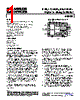


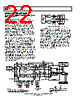


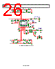


1. Overview/Introduction (Implicit)
️· This is an excerpt from the datasheet for the AD9709, which is a high-performance 14-bit digital-to-digital converter (DAC).
️· It covers key aspects like electrical characteristics, absolute maximum ratings, and pin configuration.
2. Key Features (Implicit - Features are not stated directly)
️· High-Resolution: 14-bit DAC.
️· Dual/Interleaved Operation: Supports both single and dual output configurations, implying it can function as two separate 7-bit DACs.
️· Digital Flexibility: Multiple digital input signals and control options.
️· Programmable: Includes adjustable features like gain control and sleep mode.
3. Electrical Specifications (Highlighting important values – full list is in tables)
️· Digital Inputs: Specify voltage ranges for logic levels (varying based on DVDD1/DVDD2 voltage, which can be 3.3V or 5V).
️· Output Voltage Range: Not explicitly stated in this excerpt but implied by the DAC's function.
️· Power Supply Voltages: AVDD, DVDD1, DVDD2, ACOM, DCOM1, DCOM2 (voltage ranges specified in Absolute Maximum Ratings).
️· Timing: Setup and hold times for digital inputs (Table 3).
4. Absolute Maximum Ratings
️· Voltage Ranges: Limits for all power supplies and digital input signals. Crucially, these are *absolute limits*. Exceeding them can cause permanent damage.
️· Junction Temperature: Max 150°C – vital to consider for thermal management.
️· Storage Temperature: -65°C to +150°C
️· Lead Temperature: 300°C (for soldering)
5. Pin Configuration and Function Descriptions
️· Dual Data Lines: DB0P1/DB0P2 to DB5P1/DB5P2: These are the 14 digital input bits (7 bits per channel/DAC). "P" denotes the positive signal.
️· Control Signals: Includes various control pins for configuring the DAC (e.g., SLEEP, GAINCTRL).
️· Power/Ground Pins: AVDD, DVDD1, DVDD2, ACOM, DCOM1, DCOM2: Power and ground connections.
️· Unused Pins (NC): Several pins are marked "NC" (Not Connected) – they should be left unconnected.
6. Important Tables
️· Table 6. Thermal Resistance: Provides θJA values for different package types, which are used to calculate the device's temperature rise above ambient.
️· Tables 4 and 5: Detailed specifications for voltage ranges, timing, and thermal characteristics. These are essential for proper circuit design.
What’s Missing (and Typical for an Excerpt)
️· Application Information: Circuit examples, layout recommendations, external components needed.
️· Functional Block Diagram: A visual representation of the internal architecture.
️· Detailed Timing Diagrams: More comprehensive timing diagrams for different operating modes.
️· Performance Graphs: Graphs showing DAC linearity, signal-to-noise ratio (SNR), total harmonic distortion (THD), etc.
️· Ordering Information: Part numbers, package options, temperature grades.
️· Revision History: Dates and details of changes made to the datasheet.
️· Detailed Pin Descriptions: A more thorough explanation of each pin's function.
️· Revision Number and Date: Critical for tracking updates to the datasheet.
Key Takeaways
️· The AD9709 is a high-performance 14-bit DAC with dual output capability.
️· Careful attention to absolute maximum ratings and thermal management is crucial.
️· The pin configuration and function descriptions provide a foundation for circuit design.
️· Refer to the full datasheet for complete information and application guidance.
1. Overview/Introduction (Implicit)
️· This is an excerpt from the datasheet for the AD9709, which is a high-performance 14-bit digital-to-digital converter (DAC).
️· It covers key aspects like electrical characteristics, absolute maximum ratings, and pin configuration.
2. Key Features (Implicit - Features are not stated directly)
️· High-Resolution: 14-bit DAC.
️· Dual/Interleaved Operation: Supports both single and dual output configurations, implying it can function as two separate 7-bit DACs.
️· Digital Flexibility: Multiple digital input signals and control options.
️· Programmable: Includes adjustable features like gain control and sleep mode.
3. Electrical Specifications (Highlighting important values – full list is in tables)
️· Digital Inputs: Specify voltage ranges for logic levels (varying based on DVDD1/DVDD2 voltage, which can be 3.3V or 5V).
️· Output Voltage Range: Not explicitly stated in this excerpt but implied by the DAC's function.
️· Power Supply Voltages: AVDD, DVDD1, DVDD2, ACOM, DCOM1, DCOM2 (voltage ranges specified in Absolute Maximum Ratings).
️· Timing: Setup and hold times for digital inputs (Table 3).
4. Absolute Maximum Ratings
️· Voltage Ranges: Limits for all power supplies and digital input signals. Crucially, these are *absolute limits*. Exceeding them can cause permanent damage.
️· Junction Temperature: Max 150°C – vital to consider for thermal management.
️· Storage Temperature: -65°C to +150°C
️· Lead Temperature: 300°C (for soldering)
5. Pin Configuration and Function Descriptions
️· Dual Data Lines: DB0P1/DB0P2 to DB5P1/DB5P2: These are the 14 digital input bits (7 bits per channel/DAC). "P" denotes the positive signal.
️· Control Signals: Includes various control pins for configuring the DAC (e.g., SLEEP, GAINCTRL).
️· Power/Ground Pins: AVDD, DVDD1, DVDD2, ACOM, DCOM1, DCOM2: Power and ground connections.
️· Unused Pins (NC): Several pins are marked "NC" (Not Connected) – they should be left unconnected.
6. Important Tables
️· Table 6. Thermal Resistance: Provides θJA values for different package types, which are used to calculate the device's temperature rise above ambient.
️· Tables 4 and 5: Detailed specifications for voltage ranges, timing, and thermal characteristics. These are essential for proper circuit design.
What’s Missing (and Typical for an Excerpt)
️· Application Information: Circuit examples, layout recommendations, external components needed.
️· Functional Block Diagram: A visual representation of the internal architecture.
️· Detailed Timing Diagrams: More comprehensive timing diagrams for different operating modes.
️· Performance Graphs: Graphs showing DAC linearity, signal-to-noise ratio (SNR), total harmonic distortion (THD), etc.
️· Ordering Information: Part numbers, package options, temperature grades.
️· Revision History: Dates and details of changes made to the datasheet.
️· Detailed Pin Descriptions: A more thorough explanation of each pin's function.
️· Revision Number and Date: Critical for tracking updates to the datasheet.
Key Takeaways
️· The AD9709 is a high-performance 14-bit DAC with dual output capability.
️· Careful attention to absolute maximum ratings and thermal management is crucial.
️· The pin configuration and function descriptions provide a foundation for circuit design.
️· Refer to the full datasheet for complete information and application guidance.
| Part No. | AD9709 |
| Manufacturer | AD |
| Size | 597 Kbytes |
| Pages | 32 pages |
| Description | 8-Bit, 125 MSPS, Dual TxDAC+ Digital-to-Analog Converter |
| ALLDATASHEET é útil para você? [ DONATE ] |
Sobre Alldatasheet | Publicidade | Contato conosco | Privacy Policy | Link para a ficha técnica | roca de Link | Lista de Fabricantes All Rights Reserved©Alldatasheet.com |
| Russian : Alldatasheetru.com | Korean : Alldatasheet.co.kr | Spanish : Alldatasheet.es | French : Alldatasheet.fr | Italian : Alldatasheetit.com Portuguese : Alldatasheetpt.com | Polish : Alldatasheet.pl | Vietnamese : Alldatasheet.vn Indian : Alldatasheet.in | Mexican : Alldatasheet.com.mx | British : Alldatasheet.co.uk | New Zealand : Alldatasheet.co.nz |
|
Family Site : ic2ic.com |
icmetro.com |
 Portuguese ▼
  English
 Chinese
 German
 Japanese
 Russian
 Korean
 Spanish
 French
 Italian
 Polish
 Vietnamese
 Indian
 Mexican
 British
 New Zealand