 |
Os motores de busca de Datasheet de Componentes eletrônicos |
|
|
Os motores de busca de Datasheet de Componentes eletrônicos |
|
The question interval is too short.
Please try again in a few seconds.

Hello, Please ask a question about AD9764 Datasheet
# Example questions:
➢ What is the defined measurement for total harmonic distortion (thd)?
➢ What is the purpose of the 'fs adj' pin and what external component is recommended to be connected to it?
➢ The document mentions a 'compliance range' for the dac output. what does exceeding this range potentially cause?
| Part No. | AD9764 |
| Manufacturer | AD |
| Size | 307 Kbytes |
| Pages | 22 pages |
| Description | 14-Bit, 125 MSPS TxDAC D/A Converter |






1. General Description & Function:
️· Type: Digital-to-Current Converter (DAC)
️· Core Function: Converts digital data to analog current output. It's a segmented architecture, suggesting a hierarchical design to achieve high resolution and linearity.
️· Key Outputs: Two complementary current outputs: I OUTA and I OUTB.
️· Control Inputs: Features control inputs for power down (SLEEP), reference voltage configuration (REFLO, REFIO, FS ADJ), and sleep control.
2. Key Specifications (Highlights):
️· Linearity Error: Critical performance metric - describes the deviation from an ideal linear output.
️· Differential Nonlinearity (DNL): A specific linearity metric representing the change in analog value per LSB change.
️· Offset Error: Deviation of the output from zero current.
️· Gain Error: Difference between actual and ideal output span.
️· Temperature Drift: How performance changes with temperature (offset, gain, and reference voltage drift are specified in ppm/°C).
️· Power Supply Rejection: How resistant the DAC is to power supply noise.
️· Settling Time: Time to reach a stable output.
️· Glitch Impulse: Area of undesirable output transients.
️· Spurious-Free Dynamic Range (SFDR): A measure of signal purity - how much noise and unwanted signals are present relative to the desired signal.
️· Total Harmonic Distortion (THD): A measure of harmonic distortion in the output signal.
️· Multitone Power Ratio (MPR): SFDR performance under multi-tone conditions.
3. Electrical Characteristics & Configuration:
️· Supply Voltages: DVDD & DCOM are specified (range: 2.7V to 5.5V).
️· Reference Configuration: Multiple options with REFLO and REFIO, allowing flexibility in implementing an internal or external reference.
️· Segmented Switches: Reference to segmented switches for DB13-DB5, indicating how the DAC likely achieves its performance.
️· Clock Input: Data is latched on the positive edge of the clock signal.
4. Pin Descriptions:
The datasheet excerpt provides a comprehensive listing of pin names and their respective functions (e.g., DB13-DB0 for data bits, SLEEP, REFLO, REFIO, I OUTA, I OUTB, DVDD, DCOM, CLOCK).
5. Test Setup & Diagrams
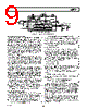
️· Figure 2 illustrates a basic AC characterization test setup.
️· It demonstrates connections to a spectrum/network analyzer.
Important Notes from the Text:
️· ESD Sensitivity: The device is ESD (Electrostatic Discharge) sensitive, requiring proper handling precautions.
️· Capacitor Requirements: Specific capacitor requirements are mentioned for reference voltage configuration and decoupling (e.g., 0.1 µF capacitors to ACOM and AVDD).
️· Architecture: The design is segmented, indicating a hierarchical approach for high resolution.
1. General Description & Function:
️· Type: Digital-to-Current Converter (DAC)
️· Core Function: Converts digital data to analog current output. It's a segmented architecture, suggesting a hierarchical design to achieve high resolution and linearity.
️· Key Outputs: Two complementary current outputs: I OUTA and I OUTB.
️· Control Inputs: Features control inputs for power down (SLEEP), reference voltage configuration (REFLO, REFIO, FS ADJ), and sleep control.
2. Key Specifications (Highlights):
️· Linearity Error: Critical performance metric - describes the deviation from an ideal linear output.
️· Differential Nonlinearity (DNL): A specific linearity metric representing the change in analog value per LSB change.
️· Offset Error: Deviation of the output from zero current.
️· Gain Error: Difference between actual and ideal output span.
️· Temperature Drift: How performance changes with temperature (offset, gain, and reference voltage drift are specified in ppm/°C).
️· Power Supply Rejection: How resistant the DAC is to power supply noise.
️· Settling Time: Time to reach a stable output.
️· Glitch Impulse: Area of undesirable output transients.
️· Spurious-Free Dynamic Range (SFDR): A measure of signal purity - how much noise and unwanted signals are present relative to the desired signal.
️· Total Harmonic Distortion (THD): A measure of harmonic distortion in the output signal.
️· Multitone Power Ratio (MPR): SFDR performance under multi-tone conditions.
3. Electrical Characteristics & Configuration:
️· Supply Voltages: DVDD & DCOM are specified (range: 2.7V to 5.5V).
️· Reference Configuration: Multiple options with REFLO and REFIO, allowing flexibility in implementing an internal or external reference.
️· Segmented Switches: Reference to segmented switches for DB13-DB5, indicating how the DAC likely achieves its performance.
️· Clock Input: Data is latched on the positive edge of the clock signal.
4. Pin Descriptions:
The datasheet excerpt provides a comprehensive listing of pin names and their respective functions (e.g., DB13-DB0 for data bits, SLEEP, REFLO, REFIO, I OUTA, I OUTB, DVDD, DCOM, CLOCK).
5. Test Setup & Diagrams
️· Figure 2 illustrates a basic AC characterization test setup.
️· It demonstrates connections to a spectrum/network analyzer.
Important Notes from the Text:
️· ESD Sensitivity: The device is ESD (Electrostatic Discharge) sensitive, requiring proper handling precautions.
️· Capacitor Requirements: Specific capacitor requirements are mentioned for reference voltage configuration and decoupling (e.g., 0.1 µF capacitors to ACOM and AVDD).
️· Architecture: The design is segmented, indicating a hierarchical approach for high resolution.
| Part No. | AD9764 |
| Manufacturer | AD |
| Size | 307 Kbytes |
| Pages | 22 pages |
| Description | 14-Bit, 125 MSPS TxDAC D/A Converter |
| ALLDATASHEET é útil para você? [ DONATE ] |
Sobre Alldatasheet | Publicidade | Contato conosco | Privacy Policy | Link para a ficha técnica | roca de Link | Lista de Fabricantes All Rights Reserved©Alldatasheet.com |
| Russian : Alldatasheetru.com | Korean : Alldatasheet.co.kr | Spanish : Alldatasheet.es | French : Alldatasheet.fr | Italian : Alldatasheetit.com Portuguese : Alldatasheetpt.com | Polish : Alldatasheet.pl | Vietnamese : Alldatasheet.vn Indian : Alldatasheet.in | Mexican : Alldatasheet.com.mx | British : Alldatasheet.co.uk | New Zealand : Alldatasheet.co.nz |
|
Family Site : ic2ic.com |
icmetro.com |
 Portuguese ▼
  English
 Chinese
 German
 Japanese
 Russian
 Korean
 Spanish
 French
 Italian
 Polish
 Vietnamese
 Indian
 Mexican
 British
 New Zealand