 |
Os motores de busca de Datasheet de Componentes eletrônicos |
|
|
Os motores de busca de Datasheet de Componentes eletrônicos |
|
The question interval is too short.
Please try again in a few seconds.

Hello, Please ask a question about AD9709 Datasheet
# Example questions:
➢ What package type is the ad9709 available in, and what is its thermal resistance (θja)?
➢ What is the maximum junction temperature (tj) specified for the ad9709?
➢ What is the typical input capacitance for the digital inputs?
| Part No. | AD9709 |
| Manufacturer | AD |
| Size | 466 Kbytes |
| Pages | 27 pages |
| Description | 8-Bit, 125 MSPS Dual TxDAC D/A Converter |


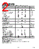


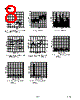
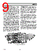
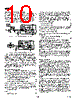





1. Device Overview & Ordering Information
️· Device: AD9709
️· Type: High-performance, mixed-signal, programmable signal path device.
️· Operating Modes: Dual and Interleaved modes.
️· Ordering Options:
- AD9709AST: -40°C to +85°C temperature range, 48-Lead LQFP package.
- AD9709-EB: Evaluation Board.
2. Absolute Maximum Ratings (These are stresses beyond which permanent damage *may* occur)
️· AVDD (with respect to ACOM): -0.3 V to +6.5 V
️· DVDD (with respect to DCOM): -0.3 V to +6.5 V
️· ACOM: -0.3 V to +0.3 V
️· Digital Inputs (with respect to DCOM): -0.3 V to +0.3 V
️· IOUTA1/IOUTA2, IOUTB1/IOUTB2: -6.5 V to +6.5 V
️· REFIO, FSADJ1, FSADJ2: -0.3 V to DVDD + 0.3 V
️· GAINCTRL, SLEEP: -0.3 V to DVDD + 0.3 V
️· Junction Temperature: -65°C to +150°C
️· Storage Temperature: -65°C to +150°C
️· Lead Temperature (10 sec): 300°C
3. Digital Input Characteristics
️· Logic “1” Voltage @ DVDD = 5V: 3.5 V
️· Logic “1” Voltage @ DVDD = 3V: 5 V
️· Logic “0” Voltage @ DVDD = 5V: 2.1 V
️· Logic “0” Voltage @ DVDD = 3V: 3 V
️· Logic “1” Current: 0 µA
️· Logic “0” Current: 1.3 µA
️· Input Capacitance: 0 pF
️· Input Setup Time (tS): -10 ns
️· Input Hold Time (tH): +10 ns
️· Latch Pulsewidth (tLPW, tCPW): 5 ns, 2.0ns, 1.5ns, 3.5ns
4. Thermal Characteristics
️· Thermal Resistance (θJA): 91°C/W
5. Key Specifications (Illustrative – a complete list would be massive)
️· AD9709AST: -40°C to +85°C temperature range
️· Evaluation Board: AD9709-EB
Important Notes and Caveats Regarding This Summary:
️· This is a summarized view: The images contain *much* more detail than what's included here. I've prioritized key parameters. This document contains an extensive amount of information.
️· Context is Crucial: Without the full datasheet and application notes, some specifications might be difficult to fully interpret.
️· "May" vs. "Will": Absolute maximum ratings are "stress" ratings. Operating the device *outside* these limits *may* cause permanent damage. It’s not a guarantee.
️· Units: Pay very close attention to the units (Volts, Amps, Ohms, degrees Celsius, etc.).
️· Illustrative Specifications: Due to the volume of data, the "Key Specifications" are just a few examples.
1. Device Overview & Ordering Information
️· Device: AD9709
️· Type: High-performance, mixed-signal, programmable signal path device.
️· Operating Modes: Dual and Interleaved modes.
️· Ordering Options:
- AD9709AST: -40°C to +85°C temperature range, 48-Lead LQFP package.
- AD9709-EB: Evaluation Board.
2. Absolute Maximum Ratings (These are stresses beyond which permanent damage *may* occur)
️· AVDD (with respect to ACOM): -0.3 V to +6.5 V
️· DVDD (with respect to DCOM): -0.3 V to +6.5 V
️· ACOM: -0.3 V to +0.3 V
️· Digital Inputs (with respect to DCOM): -0.3 V to +0.3 V
️· IOUTA1/IOUTA2, IOUTB1/IOUTB2: -6.5 V to +6.5 V
️· REFIO, FSADJ1, FSADJ2: -0.3 V to DVDD + 0.3 V
️· GAINCTRL, SLEEP: -0.3 V to DVDD + 0.3 V
️· Junction Temperature: -65°C to +150°C
️· Storage Temperature: -65°C to +150°C
️· Lead Temperature (10 sec): 300°C
3. Digital Input Characteristics
️· Logic “1” Voltage @ DVDD = 5V: 3.5 V
️· Logic “1” Voltage @ DVDD = 3V: 5 V
️· Logic “0” Voltage @ DVDD = 5V: 2.1 V
️· Logic “0” Voltage @ DVDD = 3V: 3 V
️· Logic “1” Current: 0 µA
️· Logic “0” Current: 1.3 µA
️· Input Capacitance: 0 pF
️· Input Setup Time (tS): -10 ns
️· Input Hold Time (tH): +10 ns
️· Latch Pulsewidth (tLPW, tCPW): 5 ns, 2.0ns, 1.5ns, 3.5ns
4. Thermal Characteristics
️· Thermal Resistance (θJA): 91°C/W
5. Key Specifications (Illustrative – a complete list would be massive)
️· AD9709AST: -40°C to +85°C temperature range
️· Evaluation Board: AD9709-EB
Important Notes and Caveats Regarding This Summary:
️· This is a summarized view: The images contain *much* more detail than what's included here. I've prioritized key parameters. This document contains an extensive amount of information.
️· Context is Crucial: Without the full datasheet and application notes, some specifications might be difficult to fully interpret.
️· "May" vs. "Will": Absolute maximum ratings are "stress" ratings. Operating the device *outside* these limits *may* cause permanent damage. It’s not a guarantee.
️· Units: Pay very close attention to the units (Volts, Amps, Ohms, degrees Celsius, etc.).
️· Illustrative Specifications: Due to the volume of data, the "Key Specifications" are just a few examples.
| Part No. | AD9709 |
| Manufacturer | AD |
| Size | 466 Kbytes |
| Pages | 27 pages |
| Description | 8-Bit, 125 MSPS Dual TxDAC D/A Converter |
| ALLDATASHEET é útil para você? [ DONATE ] |
Sobre Alldatasheet | Publicidade | Contato conosco | Privacy Policy | Link para a ficha técnica | roca de Link | Lista de Fabricantes All Rights Reserved©Alldatasheet.com |
| Russian : Alldatasheetru.com | Korean : Alldatasheet.co.kr | Spanish : Alldatasheet.es | French : Alldatasheet.fr | Italian : Alldatasheetit.com Portuguese : Alldatasheetpt.com | Polish : Alldatasheet.pl | Vietnamese : Alldatasheet.vn Indian : Alldatasheet.in | Mexican : Alldatasheet.com.mx | British : Alldatasheet.co.uk | New Zealand : Alldatasheet.co.nz |
|
Family Site : ic2ic.com |
icmetro.com |
 Portuguese ▼
  English
 Chinese
 German
 Japanese
 Russian
 Korean
 Spanish
 French
 Italian
 Polish
 Vietnamese
 Indian
 Mexican
 British
 New Zealand