 |
Os motores de busca de Datasheet de Componentes eletrônicos |
|
|
Os motores de busca de Datasheet de Componentes eletrônicos |
|
The question interval is too short.
Please try again in a few seconds.

Hello, Please ask a question about SP8480 Datasheet
# Example questions:
➢ What is the maximum conversion time (tc) for the adc, as specified in the datasheet?
➢ What adjustments are necessary for calibration, and what input voltages are used during these adjustments?
➢ What is the minimum low pulse width required for the r/c (read/convert) input signal?
| Part No. | SP8480 |
| Manufacturer | SIPEX |
| Size | 246 Kbytes |
| Pages | 12 pages |
| Description | Monolithic, 12-Bit Data Acquisition System |

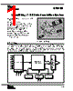


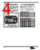


1. Overview & Features:
️· Type: 12-bit successive approximation ADC.
️· Resolution: 12-bit.
️· Throughput: Capable of converting up to 10kHz.
️· Multiplexer: Internal 8-channel multiplexer.
️· Interface: Parallel data output (8-bit wide).
️· Operation: Single supply +5V operation. Can also operate from +15V/GND.
️· Key Features:
- Low Power Consumption
- Relatively simple control/interface
- Calibration procedure for offset and gain.
- Fast Conversion Time.
- Low noise and distortion.
2. Electrical Characteristics (Key Specifications):
️· Resolution: 12 bits
️· Input Voltage Range: 0-5V (or 0-2.5V depending on configuration).
️· Conversion Time: Approximately 10µs (100kHz Sampling Rate).
️· Supply Voltage: +5V or +15V.
️· Power Dissipation: Relatively low, typically in the mW range depending on conversion rate.
️· Differential Nonlinearity: Typically 0.5 LSB.
️· Integral Nonlinearity: Typically 1.5 LSB.
️· Signal-to-Noise Ratio (SNR): Approximately 78dB (see FFT figures).
️· Total Harmonic Distortion (THD): -72dB (see FFT figures).
3. Operating Principles & Control Signals:
️· R/C (Read/Convert): This is the primary control input.
- Low Pulse: Starts a conversion cycle *and* places the output into a high-impedance state.
- High: Enables the output latches and allows data to be read.
️· A0 (Address Input): Selects either the 8 MSBs or the 4 LSBs of the converted data.
️· STATUS: Output signal indicating when a conversion is in progress or complete. It goes HIGH when conversion starts and LOW when conversion is complete and data is valid.
️· CE (Chip Enable): Enables/Disables the device for power saving and/or multi-device operation.
4. Conversion Process:
1. Start Conversion: Apply a low pulse to R/C. The device enters the conversion phase and outputs are tri-stated.
2. Conversion in Progress: STATUS goes HIGH.
3. Conversion Complete: STATUS goes LOW. The data is latched.
4. Enable Outputs: Drive R/C HIGH.
5. Select Data: Use A0 to select either MSB or LSB portion of output data.
5. Calibration Procedure:
The datasheet provides a calibration procedure to optimize the ADC's accuracy:
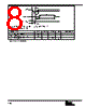
️· Offset Adjustment: Adjusts the zero-point error using a small input voltage (610µV) and observing the LSBs.
️· Gain Adjustment: Adjusts the full-scale error using a near-full-scale input voltage (4.988V) and observing the LSBs.
6. Timing Diagrams:
The datasheet includes several timing diagrams for:
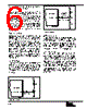
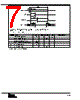
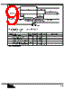
️· Low Pulse for R/C: Specifies the minimum low pulse width for starting a conversion.
️· Convert Mode Timing: Details the timing relationship between R/C, STATUS, and data output during a conversion.
️· Read Mode Timing: Specifies timing for reading data from the output latches.
7. FFT Plots:
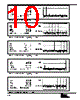
The datasheet includes FFT (Fast Fourier Transform) plots showing the ADC's noise and distortion characteristics at different input frequencies and levels. These plots demonstrate the ADC's performance and signal fidelity.
8. Applications:
Based on the specs, it is suitable for:
️· Data Acquisition Systems
️· Process Control
️· Instrumentation
️· Analog-to-Digital Conversion in general purpose applications.
️· Provide more detail on the calibration procedure.
️· Explain the meaning of the timing parameters.
️· Discuss the significance of the FFT plots.
️· Compare this ADC to other types of ADCs.
1. Overview & Features:
️· Type: 12-bit successive approximation ADC.
️· Resolution: 12-bit.
️· Throughput: Capable of converting up to 10kHz.
️· Multiplexer: Internal 8-channel multiplexer.
️· Interface: Parallel data output (8-bit wide).
️· Operation: Single supply +5V operation. Can also operate from +15V/GND.
️· Key Features:
- Low Power Consumption
- Relatively simple control/interface
- Calibration procedure for offset and gain.
- Fast Conversion Time.
- Low noise and distortion.
2. Electrical Characteristics (Key Specifications):
️· Resolution: 12 bits
️· Input Voltage Range: 0-5V (or 0-2.5V depending on configuration).
️· Conversion Time: Approximately 10µs (100kHz Sampling Rate).
️· Supply Voltage: +5V or +15V.
️· Power Dissipation: Relatively low, typically in the mW range depending on conversion rate.
️· Differential Nonlinearity: Typically 0.5 LSB.
️· Integral Nonlinearity: Typically 1.5 LSB.
️· Signal-to-Noise Ratio (SNR): Approximately 78dB (see FFT figures).
️· Total Harmonic Distortion (THD): -72dB (see FFT figures).
3. Operating Principles & Control Signals:
️· R/C (Read/Convert): This is the primary control input.
- Low Pulse: Starts a conversion cycle *and* places the output into a high-impedance state.
- High: Enables the output latches and allows data to be read.
️· A0 (Address Input): Selects either the 8 MSBs or the 4 LSBs of the converted data.
️· STATUS: Output signal indicating when a conversion is in progress or complete. It goes HIGH when conversion starts and LOW when conversion is complete and data is valid.
️· CE (Chip Enable): Enables/Disables the device for power saving and/or multi-device operation.
4. Conversion Process:
1. Start Conversion: Apply a low pulse to R/C. The device enters the conversion phase and outputs are tri-stated.
2. Conversion in Progress: STATUS goes HIGH.
3. Conversion Complete: STATUS goes LOW. The data is latched.
4. Enable Outputs: Drive R/C HIGH.
5. Select Data: Use A0 to select either MSB or LSB portion of output data.
5. Calibration Procedure:
The datasheet provides a calibration procedure to optimize the ADC's accuracy:
️· Offset Adjustment: Adjusts the zero-point error using a small input voltage (610µV) and observing the LSBs.
️· Gain Adjustment: Adjusts the full-scale error using a near-full-scale input voltage (4.988V) and observing the LSBs.
6. Timing Diagrams:
The datasheet includes several timing diagrams for:
️· Low Pulse for R/C: Specifies the minimum low pulse width for starting a conversion.
️· Convert Mode Timing: Details the timing relationship between R/C, STATUS, and data output during a conversion.
️· Read Mode Timing: Specifies timing for reading data from the output latches.
7. FFT Plots:
The datasheet includes FFT (Fast Fourier Transform) plots showing the ADC's noise and distortion characteristics at different input frequencies and levels. These plots demonstrate the ADC's performance and signal fidelity.
8. Applications:
Based on the specs, it is suitable for:
️· Data Acquisition Systems
️· Process Control
️· Instrumentation
️· Analog-to-Digital Conversion in general purpose applications.
️· Provide more detail on the calibration procedure.
️· Explain the meaning of the timing parameters.
️· Discuss the significance of the FFT plots.
️· Compare this ADC to other types of ADCs.
| Part No. | SP8480 |
| Manufacturer | SIPEX |
| Size | 246 Kbytes |
| Pages | 12 pages |
| Description | Monolithic, 12-Bit Data Acquisition System |
| ALLDATASHEET é útil para você? [ DONATE ] |
Sobre Alldatasheet | Publicidade | Contato conosco | Privacy Policy | Link para a ficha técnica | roca de Link | Lista de Fabricantes All Rights Reserved©Alldatasheet.com |
| Russian : Alldatasheetru.com | Korean : Alldatasheet.co.kr | Spanish : Alldatasheet.es | French : Alldatasheet.fr | Italian : Alldatasheetit.com Portuguese : Alldatasheetpt.com | Polish : Alldatasheet.pl | Vietnamese : Alldatasheet.vn Indian : Alldatasheet.in | Mexican : Alldatasheet.com.mx | British : Alldatasheet.co.uk | New Zealand : Alldatasheet.co.nz |
|
Family Site : ic2ic.com |
icmetro.com |
 Portuguese ▼
  English
 Chinese
 German
 Japanese
 Russian
 Korean
 Spanish
 French
 Italian
 Polish
 Vietnamese
 Indian
 Mexican
 British
 New Zealand