 |
Os motores de busca de Datasheet de Componentes eletrônicos |
|
|
Os motores de busca de Datasheet de Componentes eletrônicos |
|
The question interval is too short.
Please try again in a few seconds.

Hello, Please ask a question about HMC363 Datasheet
# Example questions:
➢ What are the key handling precautions to observe when working with the hmc363 die, and why are they important?
➢ Describe the recommended wire bonding process for the hmc363, including wire diameter and bonding parameters.
➢ Explain the functionality of the 'pwr sel' and 'pwr dwn' pins on the hmc363, and how they affect the device's operation.
| Part No. | HMC363 |
| Manufacturer | MICROSS |
| Size | 847 Kbytes |
| Pages | 9 pages |
| Description | Wide Bandwidth |


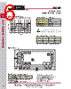
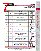
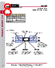

1. General Information & Description
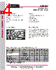
️· Product: HMC363
️· Type: GaAs HBT MMIC (Monolithic Microwave Integrated Circuit)
️· Function: Divide-by-8 Frequency Divider
️· Frequency Range: DC to 12 GHz
️· Manufacturer: Hittite Microwave (now part of Analog Devices)
️· Document Type: Datasheet
2. Electrical Characteristics
️· Supply Voltage (Vcc): 5V ± 0.25V
️· Absolute Maximum Ratings: (See datasheet for specific values on RF Input, Vcc, VLogic, Storage, Operating temperature)
️· Truth Table (Control Pins):
- DISABLE: Input buffer on/off
- PWR DWN: Device power down
- PWR SEL: High/Low power output selection
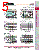
️· Typical Supply Current vs. Vcc
3. Physical Characteristics & Mounting
️· Die Size: (See outline drawing in datasheet)
️· Backside Metallization: Gold
️· Bond Pad Metallization: Gold
️· Mounting: Die attach with electrically conductive epoxy
️· Wire Bonding: Gold wire, Thermosonic bonding (specified temperatures and forces)
️· Bond Pad Spacing: 0.006 (0.150) inches
4. Functional Diagram and Pin Descriptions
️· Pin 1 (IN): RF Input (180° out of phase with Pin 3 for differential operation. AC ground for single ended operation.)
️· Pin 2 (IN): RF Input (must be DC blocked)
️· Pins 3, 4, & 5 (Vcc): Supply Voltage connection points (requires bypass capacitor).
️· Pin 6 & 7 (OUT): Divided Output signals (180° out of phase).
️· Pin 8 (PWR SEL): Power selection (low or high power output).
️· Pin 9 (PWR DWN): Device power down control.
️· Pin 10 (DISABLE): Input buffer disable control.
5. Handling & Assembly Precautions
️· Cleanliness: Handle in a clean environment. Do not use liquid cleaning systems.
️· ESD Protection: Follow ESD precautions.
️· Transient Suppression: Suppress power transients.
️· Physical Handling: Handle along edges, avoid touching surface.
6. Ordering Information
️· Contact Hittite Microwave (now Analog Devices) for price and delivery.
️· Packaging options: WP-8 (Waffle Pack) and alternates.
7. Contact Information
️· Phone: 978-250-3343
️· Fax: 978-250-3373
️· Website: www.hittite.com (now part of Analog Devices)
Important Notes:
️· This is a summary. The complete datasheet contains detailed specifications, graphs, diagrams, and information.
️· The datasheet emphasizes careful handling procedures to prevent damage.
️· Hittite Microwave is now part of Analog Devices, so ordering information and support should be directed to Analog Devices.
1. General Information & Description
️· Product: HMC363
️· Type: GaAs HBT MMIC (Monolithic Microwave Integrated Circuit)
️· Function: Divide-by-8 Frequency Divider
️· Frequency Range: DC to 12 GHz
️· Manufacturer: Hittite Microwave (now part of Analog Devices)
️· Document Type: Datasheet
2. Electrical Characteristics
️· Supply Voltage (Vcc): 5V ± 0.25V
️· Absolute Maximum Ratings: (See datasheet for specific values on RF Input, Vcc, VLogic, Storage, Operating temperature)
️· Truth Table (Control Pins):
- DISABLE: Input buffer on/off
- PWR DWN: Device power down
- PWR SEL: High/Low power output selection
️· Typical Supply Current vs. Vcc
3. Physical Characteristics & Mounting
️· Die Size: (See outline drawing in datasheet)
️· Backside Metallization: Gold
️· Bond Pad Metallization: Gold
️· Mounting: Die attach with electrically conductive epoxy
️· Wire Bonding: Gold wire, Thermosonic bonding (specified temperatures and forces)
️· Bond Pad Spacing: 0.006 (0.150) inches
4. Functional Diagram and Pin Descriptions
️· Pin 1 (IN): RF Input (180° out of phase with Pin 3 for differential operation. AC ground for single ended operation.)
️· Pin 2 (IN): RF Input (must be DC blocked)
️· Pins 3, 4, & 5 (Vcc): Supply Voltage connection points (requires bypass capacitor).
️· Pin 6 & 7 (OUT): Divided Output signals (180° out of phase).
️· Pin 8 (PWR SEL): Power selection (low or high power output).
️· Pin 9 (PWR DWN): Device power down control.
️· Pin 10 (DISABLE): Input buffer disable control.
5. Handling & Assembly Precautions
️· Cleanliness: Handle in a clean environment. Do not use liquid cleaning systems.
️· ESD Protection: Follow ESD precautions.
️· Transient Suppression: Suppress power transients.
️· Physical Handling: Handle along edges, avoid touching surface.
6. Ordering Information
️· Contact Hittite Microwave (now Analog Devices) for price and delivery.
️· Packaging options: WP-8 (Waffle Pack) and alternates.
7. Contact Information
️· Phone: 978-250-3343
️· Fax: 978-250-3373
️· Website: www.hittite.com (now part of Analog Devices)
Important Notes:
️· This is a summary. The complete datasheet contains detailed specifications, graphs, diagrams, and information.
️· The datasheet emphasizes careful handling procedures to prevent damage.
️· Hittite Microwave is now part of Analog Devices, so ordering information and support should be directed to Analog Devices.
| Part No. | HMC363 |
| Manufacturer | MICROSS |
| Size | 847 Kbytes |
| Pages | 9 pages |
| Description | Wide Bandwidth |
| ALLDATASHEET é útil para você? [ DONATE ] |
Sobre Alldatasheet | Publicidade | Contato conosco | Privacy Policy | Link para a ficha técnica | roca de Link | Lista de Fabricantes All Rights Reserved©Alldatasheet.com |
| Russian : Alldatasheetru.com | Korean : Alldatasheet.co.kr | Spanish : Alldatasheet.es | French : Alldatasheet.fr | Italian : Alldatasheetit.com Portuguese : Alldatasheetpt.com | Polish : Alldatasheet.pl | Vietnamese : Alldatasheet.vn Indian : Alldatasheet.in | Mexican : Alldatasheet.com.mx | British : Alldatasheet.co.uk | New Zealand : Alldatasheet.co.nz |
|
Family Site : ic2ic.com |
icmetro.com |
 Portuguese ▼
  English
 Chinese
 German
 Japanese
 Russian
 Korean
 Spanish
 French
 Italian
 Polish
 Vietnamese
 Indian
 Mexican
 British
 New Zealand