 |
Os motores de busca de Datasheet de Componentes eletrônicos |
|
|
Os motores de busca de Datasheet de Componentes eletrônicos |
|
The question interval is too short.
Please try again in a few seconds.

Hello, Please ask a question about UT6302G-AE3-R Datasheet
# Example questions:
➢ What is the typical drain-source breakdown voltage (bvdss) of the ut6302, as specified in the datasheet?
➢ What test conditions are used to measure the reverse recovery time (trr) of the source-drain diode in the ut6302?
➢ What is the maximum pulsed drain-source diode forward current (ism)?
| Part No. | UT6302G-AE3-R |
| Manufacturer | UTC |
| Size | 252 Kbytes |
| Pages | 5 pages |
| Description | P-CHANNEL ENHANCEMENT MOSFET |

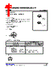
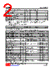
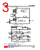
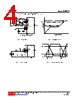

# UT6302 Power MOSFET
## Overview
️· P-Channel Enhancement Mode MOSFET
️· Ideal for portable electronics & PCMCIA cards
## Features
️· Extremely-Low On-Resistance
️· Fast Switching Speed
## Ordering Information
️· UT6302G-AE2-R: SOT-23-3 Package, Tape Reel
️· UT6302G-AE3-R: SOT-23 Package, Tape Reel
️· Pin Assignment: S=Source, G=Gate, D=Drain
## Absolute Maximum Ratings
️· Drain-Source Voltage (VDSS): -20V
️· Gate-Source Voltage (VGSS): ±12V
️· Continuous Drain Current (ID): -0.78A (at 25°C)
️· Pulsed Drain Current (IDM): -4.9A
️· Power Dissipation (PD): 540mW (derating of 4.3mW/°C above 25°C)
️· Junction Temperature (TJ): +150°C
️· Storage Temperature (TSTG): -55°C to +150°C
## Electrical Characteristics (TJ = 25°C)
️· OFF Characteristics
- Drain-Source Breakdown Voltage (BVDSS): -20V
- Drain-Source Leakage Current (IDSS): -1.0 µA
- Gate-Source Leakage Current (IGSS): ±100nA
️· ON Characteristics
- Gate Threshold Voltage (VGS(TH)): -0.70 to -1.5V
- Static Drain-Source On-Resistance (RDS(ON)): 0.60Ω (VGS=-4.5V, ID=-0.61A), 0.90Ω (VGS=-2.7V, ID=-0.31A)
️· Dynamic Parameters
- Input Capacitance (CISS): 97pF
- Output Capacitance (COSS): 53pF
- Reverse Transfer Capacitance (CRSS): 28pF
️· Switching Parameters
- Total Gate Charge (QG): 2.4-3.6nC
- Gate Source Charge (QGS): 0.56-0.84nC
- Turn-ON Delay Time (tD(ON)): 13nS
- Turn-ON Rise Time (tR): 18nS
- Turn-OFF Delay Time (tD(OFF)): 22nS
- Turn-OFF Fall-Time (tF): 22nS
️· Source-Drain Diode
- Forward Voltage (VSD): -1.2V
- Forward Current (IS): -0.54A
- Pulsed Forward Current (ISM): -4.9A
- Reverse Recovery Time (trr): 35-53nS
- Reverse Recovery Charge (QRR): 26-39nC
## Thermal Data
️· Junction to Ambient (θJA): 230°C/W (Surface Mounted on FR-4 Board)
# UT6302 Power MOSFET
## Overview
️· P-Channel Enhancement Mode MOSFET
️· Ideal for portable electronics & PCMCIA cards
## Features
️· Extremely-Low On-Resistance
️· Fast Switching Speed
## Ordering Information
️· UT6302G-AE2-R: SOT-23-3 Package, Tape Reel
️· UT6302G-AE3-R: SOT-23 Package, Tape Reel
️· Pin Assignment: S=Source, G=Gate, D=Drain
## Absolute Maximum Ratings
️· Drain-Source Voltage (VDSS): -20V
️· Gate-Source Voltage (VGSS): ±12V
️· Continuous Drain Current (ID): -0.78A (at 25°C)
️· Pulsed Drain Current (IDM): -4.9A
️· Power Dissipation (PD): 540mW (derating of 4.3mW/°C above 25°C)
️· Junction Temperature (TJ): +150°C
️· Storage Temperature (TSTG): -55°C to +150°C
## Electrical Characteristics (TJ = 25°C)
️· OFF Characteristics
- Drain-Source Breakdown Voltage (BVDSS): -20V
- Drain-Source Leakage Current (IDSS): -1.0 µA
- Gate-Source Leakage Current (IGSS): ±100nA
️· ON Characteristics
- Gate Threshold Voltage (VGS(TH)): -0.70 to -1.5V
- Static Drain-Source On-Resistance (RDS(ON)): 0.60Ω (VGS=-4.5V, ID=-0.61A), 0.90Ω (VGS=-2.7V, ID=-0.31A)
️· Dynamic Parameters
- Input Capacitance (CISS): 97pF
- Output Capacitance (COSS): 53pF
- Reverse Transfer Capacitance (CRSS): 28pF
️· Switching Parameters
- Total Gate Charge (QG): 2.4-3.6nC
- Gate Source Charge (QGS): 0.56-0.84nC
- Turn-ON Delay Time (tD(ON)): 13nS
- Turn-ON Rise Time (tR): 18nS
- Turn-OFF Delay Time (tD(OFF)): 22nS
- Turn-OFF Fall-Time (tF): 22nS
️· Source-Drain Diode
- Forward Voltage (VSD): -1.2V
- Forward Current (IS): -0.54A
- Pulsed Forward Current (ISM): -4.9A
- Reverse Recovery Time (trr): 35-53nS
- Reverse Recovery Charge (QRR): 26-39nC
## Thermal Data
️· Junction to Ambient (θJA): 230°C/W (Surface Mounted on FR-4 Board)
| Part No. | UT6302G-AE3-R |
| Manufacturer | UTC |
| Size | 252 Kbytes |
| Pages | 5 pages |
| Description | P-CHANNEL ENHANCEMENT MOSFET |
| ALLDATASHEET é útil para você? [ DONATE ] |
Sobre Alldatasheet | Publicidade | Contato conosco | Privacy Policy | Link para a ficha técnica | roca de Link | Lista de Fabricantes All Rights Reserved©Alldatasheet.com |
| Russian : Alldatasheetru.com | Korean : Alldatasheet.co.kr | Spanish : Alldatasheet.es | French : Alldatasheet.fr | Italian : Alldatasheetit.com Portuguese : Alldatasheetpt.com | Polish : Alldatasheet.pl | Vietnamese : Alldatasheet.vn Indian : Alldatasheet.in | Mexican : Alldatasheet.com.mx | British : Alldatasheet.co.uk | New Zealand : Alldatasheet.co.nz |
|
Family Site : ic2ic.com |
icmetro.com |
 Portuguese ▼
  English
 Chinese
 German
 Japanese
 Russian
 Korean
 Spanish
 French
 Italian
 Polish
 Vietnamese
 Indian
 Mexican
 British
 New Zealand